
Progress in LPE Growth of HgCdTe at Kunming Institute of Physics
-
摘要: 报道了近年来昆明物理研究所在富碲水平推舟液相外延碲镉汞外延薄膜制备技术方面的进展。2019年以来,突破了ϕ120 mm碲锌镉晶体定向生长技术,使碲锌镉衬底沉积相和夹杂相密度≤5×103 cm-2,位错腐蚀坑密度(EPD)≤4.0×104 cm-2,ϕ120 mm(111)晶圆衬底的Zn组份分布极差≤0.36%。基于碲锌镉衬底技术的进步,液相外延碲镉汞薄膜的最大生长尺寸达到了70 mm×75 mm,薄膜位错腐蚀坑密度均值为5×104 cm-2,X射线双晶回摆曲线半峰宽(DCRC-FWHM)≤35 arcsec,部分可控制到25 arcsec以下;50 mm×60 mm尺寸长波碲镉汞薄膜的厚度极差≤±1.25 μm,室温截止波长极差≤±0.1 μm,中波碲镉汞薄膜相应指标分别为≤±1 μm、≤±0.05 μm。材料技术的进展促进了制冷型碲镉汞探测器产能提升和成本的降低,也支撑了高性能长波/甚长波探测器、高工作温度(HOT)探测器以及2048×2048、4096×4096等甚高分辨率高性能探测器的研制。Abstract: The recent progress in the LPE growth of HgCdTe(MCT) epi-layer at the Kunming Institute of Physics (KIP) is reported. The precipitates and inclusion density of the CdZnTe substrate are less than 5×103 cm−2 and the etch pit density (EPD) is less than 4.0×104 cm−2. Owing to the oriented growth technology of the CdZnTe single crystal with ϕ=120 mm, the variation of the Zn components in the prepared substrate wafers with ϕ=120 mm (111) was less than 0.36%. The maximum size of the HgCdTe films grown by LPE was up to 70 mm×75 mm, with an etch pit density (EPD) of 5×104 cm−2 and DCRC-FWHM less than 35 arcsec (could be lower than 25 arcsec). Over a substrate area of 50 mm×60 mm, the thickness homogeneity of the LPE MCT epi-layer is better than Δd=±1.25 μm, and a cut-off wavelength homogeneity better than Δλ=±0.1 μm is achieved for the LWIR MCT epi-layers; that of the MWIR epi-layers are ±1 μm and ±0.05 μm, respectively. Due to the improvement of material technology, which effectively increases the yield of low-cost MCT IRFPAs at KIP, high-performance LW/VLW/HOT IRFPAs and large array detectors such as 2048×2048 and 4096×4096 based on MCT/CZT have been developed.
-
Keywords:
- liquid phase epitaxy (LPE) /
- CdZnTe substrate /
- HgCdTe (MCT) epi-layer
-
-
![]()
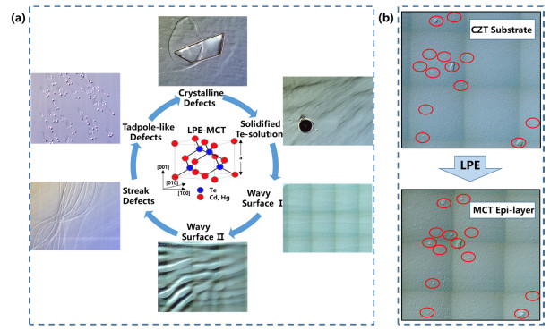
图 2 液相外延MCT薄膜主要表面缺陷类型:(a) 为外延工艺引入的缺陷;(b) 为碲锌镉衬底引入的缺陷
Figure 2. Major surface defect types of the MCT epi-layers grown by LPE, including the surface defects introduced from the LPE process (a) and derived from CZT substrates (b)
![]()
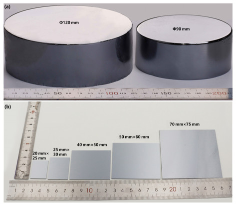
图 3 昆明物理研究所主流CZT晶锭尺寸(a)和衬底尺寸(b)
Figure 3. CZT crystal ingots (a) and substrates (b) size increase at KIP
![]()
图 4 昆明物理所碲锌镉衬底沉积相尺寸和密度的优化:(a)优化前;(b)优化后
Figure 4. Size and density decrease of precipitates and inclusion in CZT substrates at KIP: (a) Before optimization, (b) After optimization
![]()
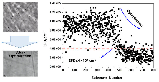
图 5 通过生长工艺优化抑制碲锌镉衬底的位错腐蚀坑密度
Figure 5. Etch pit density(EPD) of CZT substrate obtained from KIP optimized process
![]()
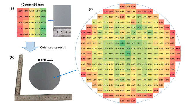
图 6 采用优化工艺后的ϕ120 mm碲锌镉晶圆Zn组分分布:(a) 优化前;(b)(c) 优化后
Figure 6. Zn content distribution over a ϕ120 mm CZT wafer made from optimized crystal growth process: (a) Before optimization; (b)(c) After optimization
![]()
图 7 70 mm×75 mm面积CZT衬底面形典型测试结果(a)和工艺优化前后衬底PV值的变化(b)
Figure 7. Measurements of topography via an optical interferometry(Zygo) (a) and the variation of PV before and after optimization (b) for 70 mm×75 mm CZT substrates
![]()
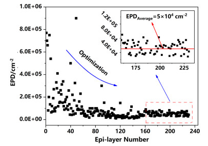
图 8 昆明物理研究所MCT外延薄膜的位错腐蚀坑密度(EPD)
Figure 8. Improvements of EPD values of MCT epi-layers grown by LPE at KIP
![]()
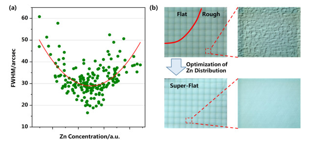
图 9 昆明物理研究所MCT薄膜半峰宽与衬底Zn组分关系(a)及50 mm×60 mm MCT薄膜表面粗糙度改善(b)
Figure 9. Mean DCRC FWHM values measured as a function of zinc content (a) and surface roughness improvements(b) of MCT epi-layers prepared at KIP
![]()
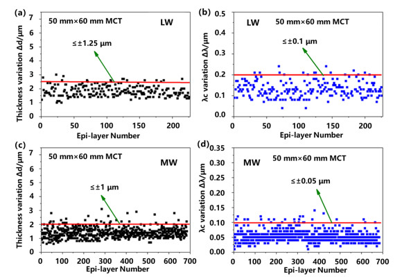
图 10 昆明物理研究所50 mm×60 mm MCT薄膜厚度和截止波长均匀性:(a)(b)长波MCT;(c)(d)中波MCT
Figure 10. Thickness and cut-off wavelength variation over the epi-layer area of 50 mm×60 mm MCT epi-layers at KIP: (a)(b)Long wavelength MCT; (c)(d) Middle wavelength MCT
![]()
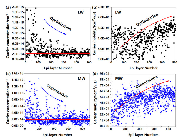
图 11 昆明物理研究所MCT薄膜材料的载流子浓度和迁移率:(a)(b)长波MCT;(c)(d)中波MCT
Figure 11. Carrier concentration and mobility measurements of hundreds of MCT epi-layers grown by LPE at KIP: (a)(b)Long wavelength MCT; (c)(d) Middle wavelength MCT
![]()
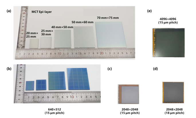
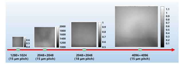
图 12 LPE MCT尺寸的增大推动了探测器生产效率的提升,单片薄膜可制备24个640×512 (15 μm pitch)芯片(a),(b);同时实现了2048×2048(15 μm pitch)、2048×2048(18 μm pitch)、4096×4096(15 μm pitch)大面阵探测器芯片的研制(c),(d),(e)
Figure 12. LPE MCT epi-layers size increase enabled up to 24 640×512(15 μm pitch)infrared arrays on one single epi-layer (a), (b); shown in (c), (d), (e) were 2048×2048(15 μm pitch), 2048×2048(18 μm pitch), 4096×4096 (15 μm pitch) infrared sensor chip assemblies(SCAs)made from KIP LPE MCT on CZT respectively
![]()
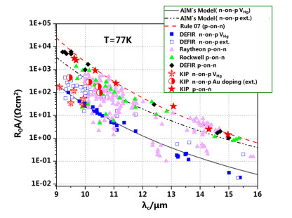
图 13 碲镉汞探测器R0A值与77 K截止波长的关系
Figure 13. MCT detector R0A product versus cutoff wavelength at 77 K, summarized with bibliographic data
![]()
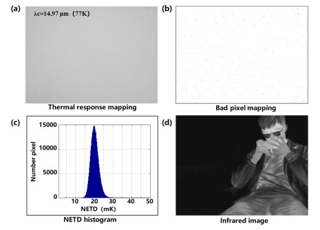
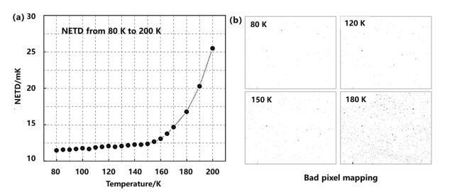
图 14 昆明物理研究所碲镉汞甚长波红外焦平面探测器性能测试结果:(a) 热响应分布图;(b) 盲元分布图;(c) NETD直方图;(d) 红外成像图[22]
Figure 14. The performance of VLWIR FPA prepared at KIP: (a) Thermal response mapping; (b) Bad pixel mapping; (c) NETD histogram; (d) Infrared image
![]()
-
[1] 杨建荣. 碲镉汞材料物理与技术[M]. 北京: 国防工业出版社, 2012. YANG Jianrong. Physics and Technology of HgCdTe Materials[M]. Beijing: National Industry Press, 2012.
[2] 宋林伟, 孔金丞, 李东升, 等. 金掺杂碲镉汞红外探测材料及器件技术[J]. 红外技术, 2021, 43(2): 97-102. http://hwjs.nvir.cn/article/id/587d68b6-af54-476a-b0b8-5a5e4ef674fd SONG Linwei, KONG Jincheng, LI Dongsheng, et al. Au-doped HgCdTe infrared material and device technology[J]. Infrared Technology, 2021, 43(2): 97-103. http://hwjs.nvir.cn/article/id/587d68b6-af54-476a-b0b8-5a5e4ef674fd
[3] Reddy M, Jin X, Lofgreen D D, et al. Demonstration of high-quality MBE HgCdTe on 8-Inch wafers[J]. Journal of Electronic Materials, 2019, 48(10): 6040-6044. DOI: 10.1007/s11664-019-07246-y
[4] Smith E P G, Venzor G M, Newton M D, et al. Inductively coupled plasma etching for large format HgCdTe focal plane array fabrication[J]. Journal of Electronic Materials, 2005, 34(6): 746-753. DOI: 10.1007/s11664-005-0014-8
[5] Bratt P R, Johnson S M, Rhiger D R, et al. Historical perspectives on HgCdTe material and device development at Raytheon Vision Systems[C]//Proceedings of SPIE, 2009, 7298: 1044-1078.
[6] Vilela Mauro F, Hogan Jack, Fennell Brian T, et al. Infinite-melt vertical liquid-phase epitaxy of HgCdTe from Hg solution: from VLWIR to SWIR[J]. Journal of Electronic Materials, 2022, 51: 4731-4741. DOI: 10.1007/s11664-022-09810-5
[7] Arkun F Erdem, Edwall Dennis D, Ellsworth Jon, et al. Characterization of HgCdTe films grown on large-area CdZnTe substrates by molecular beam epitaxy[J]. Journal of Electronic Materials, 2017, 46(9): 5374-5378. DOI: 10.1007/s11664-017-5441-9
[8] Mosby G, Rauscher B J, Bennett C, et al. Properties and characteristics of the Nancy Grace Roman Space Telescope H4RG-10 detectors[J]. Journal of Astronomical Telescopes Instruments and Systems, 2020, 6(4): DOI: 10.1117/1.JATIS.6.4.046001.
[9] Atkinson D, Bezawada N, Hipwood L G, et al. Operation and performance of new NIR detectors from SELEX[C]//Proceedings of SPIE, 2012, 8453: 84530U.
[10] Santailler Jean-Louis, Gout Erik, Journot Timotée, et al. From 5" CdZnTe ingots to high quality (111) CdZnTe substrates for SWIR 2k2 15 µm pitch infrared focal plane arrays manufacturing[C]//Proceedings of SPIE, 2020: DOI: 10.1117/12.2561377.
[11] Lovecchio P, Wong K, Parodos T, et al. Advances in liquid phase epitaxial growth of Hg1-xCdxTe for SWIR through VLWIR photodiodes [C]//Proceedings of SPIE, 2004, 5564: 65-72.
[12] Wenisch J, Bitterlich H, Bruder M, et al. Large-format and long-wavelength infrared mercury cadmium telluride detectors[J]. Journal of Electronic Materials, 2013, 42(11): 3186-3190. DOI: 10.1007/s11664-013-2757-y
[13] 孙权志, 孙瑞赟, 魏彦锋, 等. 50 mm×50 mm高性能HgCdTe液相外延材料的批生产技术[J]. 红外与毫米波学报, 2017, 36(1): 49-54. https://www.cnki.com.cn/Article/CJFDTOTAL-HWYH202102010.htm SUN Quanzhi, SUN Ruiyun, WEI Yanfen, et al. Batch production technology of 50 mm×50 mm HgCdTe LPE materials with high performance[J]. Journal of Infrared and Millimeter Waves, 2017, 36(1): 49-54. https://www.cnki.com.cn/Article/CJFDTOTAL-HWYH202102010.htm
[14] 刘伟华, 刘帆, 吴正虎, 等. 12 μm像元间距1280×1024碲镉汞中波红外焦平面探测器的制备及性能研究[J]. 红外, 2020, 41(3): 9-15. https://www.cnki.com.cn/Article/CJFDTOTAL-HWAI202003002.htm LIU Weihua, LIU Fan, WU Zhenghu, et al. Study on preparation and performance of 1280×1024@12 μm HgCdTe MWIR focal plane detectors[J]. Infrared, 2020, 41(3): 9-15. https://www.cnki.com.cn/Article/CJFDTOTAL-HWAI202003002.htm
[15] 高达, 李震, 王丹, 等. 大尺寸碲锌镉基碲镉汞材料分子束外延技术研究[J]. 激光与红外, 2022, 52(3): 388-391. https://www.cnki.com.cn/Article/CJFDTOTAL-JGHW202203013.htm GAO Da, LI Zhen, WANG Dan, et al. Research on molecular beam epitaxy growth of HgCdTe large CdZnTe substrate[J]. Laser & Infrared, 2022, 52(3): 388-391. https://www.cnki.com.cn/Article/CJFDTOTAL-JGHW202203013.htm
[16] Koyama A, Hichiwa A, Hirano R. Recent progress in CdZnTe craystal[J]. Journal of Electronic Materials, 1999, 28(6): 683-687. DOI: 10.1007/s11664-999-0054-6
[17] 袁绶章, 赵文, 孔金丞, 等. Cd饱和气氛退火对碲锌镉晶体导电类型转变界面的影响[J]. 红外技术, 2021, 43(6): 517-522. http://hwjs.nvir.cn/article/id/ebc94562-b5eb-4803-b866-53a3ed83d591 YUAN Shouzhang, ZHAO Wen, KONG Jincheng, et al. Influence of Cd-rich annealing on position-dependent conductivity transition in Cd1-xZnxTe crystal[J]. Infrared Technology, 2021, 43(6): 517-522. http://hwjs.nvir.cn/article/id/ebc94562-b5eb-4803-b866-53a3ed83d591
[18] 赵文, 孔金丞, 姜军, 等. Cd1-xZnxTe晶体中由本征缺陷引起的导电类型转变界面研究[J]. 红外技术, 2022, 44(6): 560-564. http://hwjs.nvir.cn/article/id/b83b7360-956e-4770-9595-8b1658deaa0b ZHAO Wen, KONG Jincheng, JIANG Jun, et al. Position-dependent conductivity transition by intrinsic defects in Cd1-xZnxTe crystal[J]. Infrared Technology, 2022, 44(6): 560-564. http://hwjs.nvir.cn/article/id/b83b7360-956e-4770-9595-8b1658deaa0b
[19] 袁绶章, 赵文, 孔金丞, 等. 原位退火对碲锌镉晶体第二相夹杂缺陷的影响[J]. 红外技术, 2021, 43(7): 615-621. http://hwjs.nvir.cn/article/id/92499484-e5a1-4255-858b-0af603887888 YUAN Shouzhang, ZHAO Wen, KONG Jincheng, et al. Effect of in-situ post-annealing on the second phase inclusion defects[J]. Infrared Technology, 2021, 43(7): 615-621. http://hwjs.nvir.cn/article/id/92499484-e5a1-4255-858b-0af603887888
[20] Cathignol A, Brellier D, Gout E, et al. From CdZnTe bulk growth to HgCdTe infra-red detectors: mastering the chain for high-performance and reliable imaging[C]//Proceedings of SPIE, 2018, 10624, DOI: 10.1117/12.2304950.
[21] 龚晓丹, 李红福, 杨超伟, 等. 大面阵短波碲镉汞红外焦平面器件研究[J]. 红外与激光工程, 2022, 51(9): DOI: 10.3788/IRLA20220079. GONG Xiaodan, LI Hongfu, YANG Chaowei, et al. Study on large-area array SW HgCdTe infrared focal plane device[J]. Infrared and Laser Engineering, 2022, 51(9): DOI: 10.3788/IRLA20220079.
[22] 李立华, 熊伯俊, 杨超伟, 等. P-on-n长波、甚长波碲镉汞红外焦平面器件技术研究[J]. 红外与毫米波学报, 2022, 41(3): 534-539. https://www.cnki.com.cn/Article/CJFDTOTAL-HWYH202203001.htm LI Lihua, XIONG Bojun, YANG Chaowei, et al. Research on p-on-n LWIR and VLWIR HgCdTe infrared focal plane detectors technology[J]. Journal of Infrared and Millimeter Waves, 2022, 41(3): 534-539. https://www.cnki.com.cn/Article/CJFDTOTAL-HWYH202203001.htm
[23] Wollrab R, Bauer A, Bitterlich H, et al. Planar n-on-p HgCdTe FPAs for LWIR and VLWIR applications[J]. Journal of Electronic Materials, 2011, 40(8): 1618-1623.
[24] Tennant W E, Lee Donald, Zandian Majid, et al. MBE HgCdTe technology: a very general solution to IR detection, described by "Rule 07", a very convenient heuristic[J]. Journal of Electronic Materials, 2008, 37(9): 1406-1410.
[25] 陈军, 习中立, 秦强, 等. 碲镉汞高温红外探测器组件进展[J]. 红外与激光工程, 2023, 52(1), DOI: 10.3788/IRLA20220462. CHEN Jun, XI Zhongli, QIN Qiang, et al. Advance in high operating temperature HgCdTe infrared detector[J]. Infrared and Laser Engineering, 2023, 52(1): DOI: 10.3788/IRLA20220462.
 下载:
下载:


计量
- 文章访问数: 422
- HTML全文浏览量: 213
- PDF下载量: 214
