
Effect of Annealing on C-V Characteristics of InSb Metal-Insulator-Semiconductor Devices
-
摘要: 采用原子层沉积技术制备Al2O3薄膜作为InSb材料介电层,制备了MIS器件,研究了金属化后不同退火温度对界面特性的影响。利用C-V测试表征了MIS(metal-insulator-semiconductor)器件的界面特性,结果表明Al2O3介电层引入了表面固定正电荷,200℃和300℃退火处理可有效减小慢界面态密度,利用Terman法得到了禁带界面态密度分布,表明200℃退火可使禁带中央和导带附近的界面态密度显著减小。同时文章对C-V曲线滞回的原因进行了分析,认为Al2O3介电层中离界面较近的负体陷阱电荷是主要影响因素。实验证明了200℃~300℃的退火处理可有效改善InSb/Al2O3界面质量。Abstract: An Al2O3 film was prepared as a dielectric layer for an InSb material via the atomic layer deposition technique, the MIS device was developed, and the effects of annealing temperature on the post-metallization interfacial characteristics were investigated. Moreover, the interface of the MIS device was characterized using the C-V test. The results indicate that the Al2O3 dielectric layer introduced surface-fixed positive charges, and annealing processing at 200 and 300℃ can effectively reduce the slowing density. Furthermore, Terman's method can be used to obtain the interface states density distribution. This indicates that 200℃ annealing can significantly decrease the interfacial density close to the center of the bandgap and the conduction band. Additionally, negative charges being trapped near the interface of the Al2O3 dielectric layer is found to be the main cause of C-V curve hysteresis. Experiments prove that an annealing process at 200℃−300℃ can effectively improve the InSb/Al2O3 interface quality.
-
Keywords:
- Indium Antimonide /
- C-V /
- post metalization annealing /
- atomic layer deposition
-
-
![]()
![]()
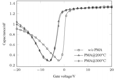
图 3 不同退火温度下C-V曲线的滞回特性(实线表示从反型区开始扫描,虚线表示从积累区开始扫描)
Figure 3. Hysteresis C-V curves at different annealing temperature (Solid line denotes scanning from the inversion region, dotted line denotes scanning from the accumulation region)
![]()
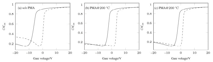
图 4 不同扫描方向和起始偏压的C-V曲线:(a) 从积累区开始扫描;(b) 从反型区开始扫描
Figure 4. C-V curves with different scanning directions and initial bias: (a) Scan from the accumulation region; (b) Scan from the inversion region
![]()
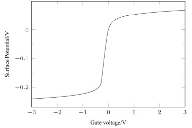
图 6 理想栅电压与表面势的关系曲线
Figure 6. Ideal relationship curve of gate voltage and surface potential
![]()
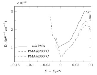
图 7 界面态密度在禁带中的分布(相对于本征费米能级Ei)
Figure 7. Interface state density as a function of energy in the bandgap(relative to the intrinsic Fermi level Ei)
表 1 样品对应的退火条件
Table 1 Annealing conditions corresponding to the sample
Sample Annealing conditions #1 Without annealing(w/o PMA) #2 200℃, 5 min(PMA@200℃) #3 300℃, 5 min(PMA@300℃)  下载: 导出CSV
表 2 不同退火条件的平带电压及对应的固定电荷的大小
Table 2 Flat band voltage and fixed surface charge density at different annealing conditions
w/o PMA PMA
@200℃PMA
@300℃VFB/V 0.82 −3.2 −3 Qf /cm−2 −8.4716×10¹¹ 2.8823×10¹² 2.7466×10¹²
下载: 导出CSV
表 3 不同退火条件的滞回电压及慢界面态密度
Table 3 Voltage hysteresis and slow interface states density at different annealing conditions
w/o PMA PMA
@200℃PMA
@300℃VFB/V 6.75 5.8 3.6 Ntrap/cm−2 4.2×10¹² 3.6×10¹² 2.2×10¹²
下载: 导出CSV
-
[1] 周冠山. 光伏型锑化铟红外探测器零偏结阻抗结面积乘积的分析[J]. 航空兵器, 1999(1): 10-17. https://www.cnki.com.cn/Article/CJFDTOTAL-HKBQ199901003.htm ZHOU G S. Analysis of zero bias junction impedance and junction area product of photovoltaic InSb infrared detector[J]. Aero Weaponry, 1999(1): 10-17 https://www.cnki.com.cn/Article/CJFDTOTAL-HKBQ199901003.htm
[2] Bennett B R, Ancona M G, Boos J B. Compound semiconductors for low-power p-channel field-effect transistors[J]. MRS Bulletin, 2009, 34(7): 530-536. DOI: 10.1557/mrs2009.141
[3] Pawlowski J, Szumniak P, Bednarek S. Electron spin rotations induced by oscillating Rashba interaction in a quantum wire[J]. Physical Review B, 2016, 93(4): 045309. DOI: 10.1103/PhysRevB.93.045309
[4] CHEN Y, HUANG S, PAN D, et al. Strong and tunable spin-orbit interaction in a single crystalline InSb nanosheet[J]. Npj 2D Materials and Applications, 2021, 5(1): 1-8. DOI: 10.1038/s41699-020-00190-0
[5] 常虎东. 高迁移率InGaAs沟道MOSFET器件研究[D]. 北京: 中国科学院大学, 2013. CHANG H D. Research on High Mobility InGaAs Channel MOSFET Devices[D]. Beijing: University of Chinese Academy of Sciences, 2013.
[6] Trinh H D, Nguyen M T, Lin Y C, et al. Band alignment parameters of Al2O3/InSb metal-oxide-semiconductor structure and their modification with oxide deposition temperatures[J]. Applied Physics Express, 2013, 6(6): 1-3.
[7] Black L E. New Perspectives on Surface Passivation: Understanding the Si-Al2O3 Interface[D]. Canberra: The Australian National University, 2015.
[8] Baik M, Kang H K, Kang Y S, et al. Electrical properties and thermal stability in stack structure of HfO2/Al2O3/InSb by atomic layer deposition[J]. Scientific Reports, 2017, 7(1): 1-11. DOI: 10.1038/s41598-016-0028-x
[9] Kim H S, Ok I, ZHANG M, et al. A study of metal-oxide-semiconductor capacitors on GaAs, In0.53Ga0.47As, InAs, and InSb substrates using a germanium interfacial passivation layer[J]. Applied Physics Letters, 2008, 93(6): 062111. DOI: 10.1063/1.2972107
[10] Vavasour O J, Jefferies R, Walker M, et al. Effect of HCl cleaning on InSb-Al2O3 MOS capacitors[J]. Semiconductor Science and Technology, 2019, 34(3): 035032. DOI: 10.1088/1361-6641/ab0331
[11] Luc Q H, CHANG E Y, Trinh H D, et al. Effect of annealing processes on the electrical properties of the atomic layer deposition Al2O3/In0.53Ga0.47As metal oxide semiconductor capacitors[J]. Japanese Journal of Applied Physics, 2014, 53(4S): 04EF04. DOI: 10.7567/JJAP.53.04EF04
[12] Vavasour O J. Dielectrics for Narrow Bandgap Ⅲ-Ⅴ Devices[D]. Coventry: University of Warwick, 2018.
[13] Winter R, Ahn J, Mcintyre P C, et al. New method for determining flat-band voltage in high mobility semiconductors[J]. Journal of Vacuum Science & Technology B Microelectronics & Nanometer Structures, 2013, 31(3): 0604.
[14] McNutt M, Sah C T. Determination of the MOS oxide capacitance[J]. Journal of Applied Physics, 1975, 46(9): 3909-3913. DOI: 10.1063/1.322138
[15] Walstra S V, Sah C T. Extension of the McNutt-Sah method for measuring thin oxide thicknesses of MOS devices[J]. Solid State Electronics, 1998, 4(42): 671-673.
[16] Maserjian J, Petersson G, Svensson C. Saturation capacitance of thin oxide MOS structures and the effective surface density of states of silicon[J]. Solid-state Electronics, 1974, 17: 335-339. DOI: 10.1016/0038-1101(74)90125-7
[17] Riccò B, Olivo P, Nguyen T, et al. Oxide-thickness determination in thin-insulator MOS structures[J]. IEEE Transactions on Electron Devices, 1988, 35(4): 432-438. DOI: 10.1109/16.2476
[18] WEI D. Study of High Dielectric Constant Oxides on GaN for Metal Oxide Semiconductor Devices[D]. Manhattan: Kansas State University, 2014.
[19] Lee W C, Cho C J, Choi J H, et al. Correct extraction of frequency dispersion in accumulation capacitance in InGaAs metal-insulator -semiconductor devices[J]. Electronic Materials Letters, 2016, 12(6): 768-772. DOI: 10.1007/s13391-016-6226-7
[20] Taoka N, Yokoyama M, Kim S H, et al. Influence of interface traps inside the conduction band on the capacitance-voltage characteristics of InGaAs metal-oxide-semiconductor capacitors[J]. Applied Physics Express, 2016, 9(11): 111202. DOI: 10.7567/APEX.9.111202
-
期刊类型引用(9)
1. 王雁,吕琴红,杨卫,董永谦. 全闭环柔性填网工艺在红外器件组装中的应用. 电子工艺技术. 2024(01): 28-30 .  百度学术
百度学术
2. 朱海勇,曾智江,孙闻,赵振力,范广宇,季鹏,张启,庄馥隆,李雪. 冷光学用大口径2 k×2 k红外探测器组件封装技术. 红外与激光工程. 2024(05): 81-90 . 百度学术
3. 李振雷,谢萌,饶启超,韩蓬磊. 分置式斯特林制冷机耦合间隙对探测器性能的影响. 红外. 2024(06): 42-47 . 百度学术
4. 江乐果,潘凯,田雯,王一波,赵海兴. 基于高压制冷的光电吊舱降噪优化研究. 红外技术. 2024(11): 1347-1353 . 本站查看
5. 张永壮,龚志红,饶启超,卢旭辰,韩蓬磊,温建国,耿利红. 斯特林制冷机驱动器元器件的散热优化设计及试验研究. 红外. 2023(07): 34-38 . 百度学术
6. 江晨,丁森,朱鲲捷,胡攀辉,陈风,吴丹,郁佳敏. 高压气瓶结构设计与仿真及试验研究. 机械制造与自动化. 2023(05): 181-184 . 百度学术
7. 江晨,陈风,丁森,胡圣鑫,郁佳敏,江春月,吴君辉. 高压制冷气瓶的轻量化设计与分析. 机械制造. 2022(03): 25-26+36 . 百度学术
8. 苏永强. 金属C型密封圈在斯特林制冷机中的应用. 红外技术. 2022(07): 757-762 . 本站查看
9. 辛存良,程多文,杨坤,傅斌. 聚四氟乙烯基耐磨涂层在制冷机中的试验分析. 低温与超导. 2020(07): 29-32 . 百度学术
其他类型引用(1)
计量
- 文章访问数:
- HTML全文浏览量:
- PDF下载量:
- 被引次数: 10
