
The Research Progress in Type Ⅱ Superlattices Infrared Focal Plane Array Detectors
-
摘要: 近几年,二类超晶格红外探测器在材料生长、器件结构设计、器件制备上经历了快速的发展,使得二类超晶格成为除碲镉汞外最受关注的红外探测器材料。本文简要介绍了二类超晶格的优势,总结了国际上二类超晶格红外探测器研究进展,回顾了二类超晶格红外探测器的技术发展历程,并分析了国内二类超晶格材料与器件中存在的技术问题。Abstract: In recent years, the type Ⅱ superlattices (T2SL) infrared detector has experienced incredible improvements in material growth, device structure design, device fabrication techniques, which make the T2SL become the most popular infrared detector material, besides HgCdTe. This article briefly introduces the advantage of the T2SL material, summarizes the international research status in T2SL-based photodetectors, reviews the history of technology development of T2SL-based photodetectors and analyzes the drawback of the research of T2SL material and device technology in China.
-
Keywords:
- type Ⅱ superlattices /
- infrared detector /
- focal-plane arrays (FPAs)
-
0. 引言
二类超晶格的概念由IBM研究院的Sai-Halasz和Esaki等科学家于1977年提出[1],随后他们对InAs/GaSb二类超晶格的能带结构进行了理论计算[2],根据计算结果:InAs/GaSb超晶格根据其周期结构厚度的不同,表现出半导体特性或半金属特性。InAs/GaSb二类超晶格被提出以来,即在红外探测应用上引起了极大的兴趣。1987年,Smith和Mailhiot[3]发表了InAs/GaSb二类超晶格作为红外探测器的理论性能预测,极大地推动了InAs/GaSb二类超晶格作为红外探测器材料的研究。1996年,Johnson J. L.等人[4]制作成第一支InAs/GaSb超晶格二极管开启了二类超晶格红外探测器研究的时代。经过近30年的发展,基于二类超晶格的红外探测器在材料制备、器件结构设计、器件制备工艺上都取得了不错的进展[5-6]。
为了红外探测器研究领域更好地了解二类超晶格材料与二类超晶格红外探测器的研究进展,本文介绍了二类超晶格材料作为红外探测器的优势,国际上二类超晶格红外焦平面探测器的研究进展与技术发展历程,并分析国内二类超晶格红外探测器材料与器件研究中存在的技术问题。关于二类超晶格红外探测器技术的介绍详见文献[7-8],本文不再赘述。
1. 二类超晶格材料及其作为红外探测器的优势
以InAs/GaSb超晶格为例简单介绍二类超晶格材料。使得这个材料体系在红外探测领域受到关注的重要特征便是它在InAs和GaSb界面处二类能带排列形式,InAs/GaSb异质结在能带排列表现出二类错排式(broken gap):在界面处,InAs的导带底要比GaSb的价带顶底高150 meV,在带隙上表现出一种错排的形式,如图 1所示。在这样一种异质结中,InAs的导带和GaSb的价带存在部分交叠,电子和空穴被分别分离限制在异质界面两侧不同的量子阱中。InAs/GaSb超晶格由超薄的InAs层与GaSb层周期性地交替生长构成,超晶格超薄层结构使得材料中的电子和空穴不能被限制在其中某一个量子阱中,电子和空穴通过势垒隧穿形成微带,如图 1所示。二类超晶格这种特殊的能带结构使其可以表现为不同于组成材料的性质,其有效带隙可以通过周期厚度灵活调节。理论计算结果显示二类超晶格有效带隙可以从0连续调节到400 meV,具有覆盖3.1~30 μm波段红外探测能力。
二类超晶格材料独特的能带结构使得它具有如下优势:
1)俄歇复合抑制。俄歇复合是红外探测器在高温工作情况下的主要限制因素,对于二类超晶格材料来说俄歇复合可以通过对能带结构的调控加以抑制。
2)载流子有效质量大。相比于碲镉汞和其它窄禁带半导体,二类超晶格由于其特殊的能带结构,载流子有效质量相对较大(对于长波材料来说,二类超晶格电子有效质量约为0.03m0,碲镉汞电子有效质量约为0.009m0)。大的有效质量可以降低探测器的隧穿电流,而隧穿电流在长波和甚长波碲镉汞红外探测器的暗电流中起主要贡献。
3)能带灵活可调。除了有效带隙可以在0~400 meV连续可调,覆盖3.1~30 μm波段红外探测能力外。二类超晶格材料的带边(导带底和价带顶)可以独立调节,为新型器件结构(特别是势垒型器件)设计开发提供了平台,这对于三元化合物半导体(比如碲镉汞)来说是难以想象的。
4)均匀性好。二类超晶格材料的电子结构通过组成材料的周期厚度来控制,从分子束外延生长的角度来讲,是由三族元素的撞击速率决定,并不随生长温度和束流比变化。相比于三元化合物(碲镉汞)的摩尔组分控制,二类超晶格材料的周期厚度控制对生长条件的依赖性更小,从而可以达到更好的均匀性。
5)带间跃迁,不受光学跃迁选择定则限制,吸收系数与碲镉汞材料相当。不像量子阱材料通过子带间跃迁实现红外辐射的探测,二类超晶格材料属于带间跃迁,不受跃迁选择定则限制,可以吸收正入射的红外辐射,而且吸收系数与碲镉汞材料相当。
相比于量子阱探测器,超晶格探测器不存在跃迁选择定则的限制,可以吸收正入射光,不需要制备复杂的光栅结构。另外,超晶格红外探测器的量子效率也要高于量子阱。由于量子效率低,量子阱探测器只能通过延长积分时间来提高性能,而延长积分时间又会使得暗电流对积分电容的贡献增大,因此量子阱红外探测器只能工作在较低的温度,量子阱探测器一般工作在65~73 K。因此,超晶格红外探测器相对于量子阱红外探测器有明显的优势。
相比于碲镉汞红外探测器,现阶段的超晶格红外探测器在量子效率和暗电流上都稍逊于碲镉汞。由于超晶格探测器的研制还处于较早的时期(或关键时期),如果能在材料生长、器件结构设计和焦平面制备工艺上等方面有突破,很有希望可以赶上碲镉汞。另外,超晶格探测器在有效像元率(operability)、空间均匀性(spatial uniformity)、时间稳定性(temporal stability)、可制造性(producibility)和成本上(affordability)要比碲镉汞有优势,称为“ility优势”。二类超晶格材料的这些优势使得它成为开发第三代红外探测器重点关注的材料。
2. 二类超晶格红外探测器研究进展
由于二类超晶格探测器在材料、器件物理以及器件性能方面显示出的优异特性,现已成为当前国际上红外探测器研究的热点,世界上许多国家都开展了对二类超晶格材料及其器件的研究,并取得了快速的发展。当前,国际上较为领先的研究机构有美国的西北大学(Northwestern University)量子器件中心(Center for Quantum devices,CQD)、喷气推进实验室(Jet Propulsion Laboratory, JPL)、休斯实验室(Hughes Research Laboratories, HRL),德国弗朗霍夫协会应用固体物理研究所(Fraunhofer-Institutfür Angewandte Festkörperphysik, IAF)和AIM公司(Infrarot-Module GmbH),以色列的SCD公司(SemiConductor Device)。他们对材料生长、器件机理和焦平面探测器研制等进行了全面研究,目前已突破了高量子效率的生长技术。本文将介绍这些研究机构在二类超晶格中波、长波、双色(主要是中中双色和中长双色)红外焦平面探测器的研究进展。
2.1 中波红外焦平面探测器
中波红外探测器是响应波长在3~5 μm之间的红外探测器。中波红外探测器可以用于不同场合,比如:航空、卫星侦查,目标追踪,航海技术,目标识别等。
德国IAF和AIM是最早实现InAs/GaSb二类超晶格中波红外焦平面探测器的研究机构。早在2005年,IAF和AIM就报道了他们第一个二类超晶格中波红外焦平面探测器的结果[9]。探测器吸收层超晶格设计为9.5 MLs/12 MLs的InAs/GaSb,器件结构为普通的n-i-p二极管结构,如图 2所示。单元器件测试结果表明,探测器在77 K下的5%截止波长为5.4 μm,R0A为4×10⁵ Ω·cm2,量子效率30%。焦平面规模为256×256,像元中心距40 μm,在77 K、5 ms及f/2测试条件下,NETD为11.1 mK,失效像元(短路,开路以及NETD超过100 mK)占1%~2%。图 3为红外焦平面相机的成像效果[9],图 3(a)毛衣的精细结构表明焦平面探测器具有好的调制传递函数(Modulation Transfer Function,MTF);图 3(b)中看到的血管证实了红外焦平面探测器约10 mK的噪声等效温差(noise equivalent temperature difference,NETD)。2006年,IAF和AIM[10]将焦平面探测器规模扩大为384×288,像元中心距减小到24 μm,芯片的尺寸缩小了36%,大小为10.14 mm×7.9 mm,所以每个2英寸wafer上可以制备8个焦平面器件。同时,通过增加超晶格周期数的方法提高了器件的量子效率。超晶格周期数从原来的190个周期增加到370个周期,其量子效率提高了大约一倍。
![]() 图 2 AIM InAs/GaSb超晶格中波二极管截面示意图Figure 2. Schematic cross section of an InAs/GaSb SL MWIR diode of AIM
图 2 AIM InAs/GaSb超晶格中波二极管截面示意图Figure 2. Schematic cross section of an InAs/GaSb SL MWIR diode of AIM![]() 图 3 AIM InAs/GaSb超晶格256×256中波焦平面成像系统拍摄的照片Figure 3. Thermal images taken with the InAs/GaSb superlattice 256×256 MWIR FPA camera system of AIM
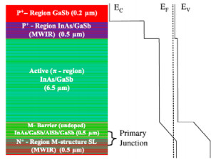
图 3 AIM InAs/GaSb超晶格256×256中波焦平面成像系统拍摄的照片Figure 3. Thermal images taken with the InAs/GaSb superlattice 256×256 MWIR FPA camera system of AIM国际上,二类超晶格中波红外探测器研制较为领先的机构还有美国西北大学。他们的目标是研制工作温度高于150 K的中波高温探测器。他们提出了一种新型势垒型器件结构p-π-M-N来实现高温工作,其中吸收层π采用传统的InAs/GaSb二类超晶格,M和N采用M结构(InAs/GaSb/AlSb/GaSb)超晶格。能带排列上,M结构超晶格与吸收区的InAs/GaSb超晶格在导带上连续,而在价带上存在较大的带阶。这样的结构,相比于普通p-n结二极管,可以抑制暗电流,同时不产生量子效率的偏压依赖。2011年,他们报道了利用p-π-M-N器件结构研制的中波高温探测器[11]。单元器件结果表明,150 K下,50%截止波长为4.2 μm,R0A为5100 Ω·cm2,探测率为1.05×10¹² Jones。探测率变温测试结果表明直到180 K,器件依旧是背景限制性能,相比于同质结器件提高了25K。他们利用p-π-M-N器件结构制作了320×256中波高温红外焦平面探测器,并将探测器芯片与Indigo ISC9705读出电路互连。焦平面探测器在120 K和150 K下的成像效果如图 4(a)和(b)所示。焦平面测试结果表明,f/2.3,10.02 ms积分时间,以及120 K测试条件下,焦平面NETD为11 mK,如图 4(c)所示。130~150 K工作温度下,随着温度升高,NETD升高,是因为暗电流的增加。为了避免因为暗电流提高使得读出电路中电容饱和,130~150 K工作温度下,积分时间减小到4.02 ms。
![]() 图 4 美国西北大学中波焦平面探测器在120 K(a)和150 K(b)下的成像照片,(c) 86-150 K下焦平面的NTEDFigure 4. Images taken with a MWIR FPA detector of Northwestern University operating at (a) 120 K and (b) 150 K (c) NEDT measured from 86 to150 K
图 4 美国西北大学中波焦平面探测器在120 K(a)和150 K(b)下的成像照片,(c) 86-150 K下焦平面的NTEDFigure 4. Images taken with a MWIR FPA detector of Northwestern University operating at (a) 120 K and (b) 150 K (c) NEDT measured from 86 to150 K休斯实验室作为美国VISTA计划(Vital Infrared Sensor Technology Acceleration,关键红外传感器技术加速计划)的红外焦平面探测器制备机构,2017年报道了1k×2k/5 μm超晶格高温中波红外焦平面探测器的研究进展[12]。文中未报道具体材料和器件结构,仅报道了焦平面探测器性能。150 K下,焦平面探测器的开启电压为-150 mV,截止波长5.1 μm,暗电流为6.3×10⁻⁶ A/cm-2,量子效率约60%,有效像元率为99.9%,f/2.3冷屏和帧平均条件下,NETD小于20 mK。焦平面的成像演示照片,如图 5所示。
![]() 图 5 休斯实验室1 k×2 k/5 μm焦平面在150 K下拍摄的照片Figure 5. Image captured by a 1 k×2 k/5 μm MWIR FPA of HRL operated at 150 K
图 5 休斯实验室1 k×2 k/5 μm焦平面在150 K下拍摄的照片Figure 5. Image captured by a 1 k×2 k/5 μm MWIR FPA of HRL operated at 150 K2018年,JPL也对其二类超晶格中波高温红外焦平面探测器进行了报道[13-14]。JPL同样是超晶格红外焦平面探测器研究领域较为领先的研究机构,在材料生长、器件设计与制备方面都有着非常丰富的经验。JPL的超晶格中波红外探测器采用的是InAs/InAs0.66Sb0.33超晶格作为吸收层的nBn势垒型探测器,JPL将其称为HOT-BIRD[14]。单元器件结果表明,150 K工作温度下,截止波长约5.4 μm,暗电流密度约4.5×10⁻⁵ A/cm-2,量子效率约52%(4.5 μm,无抗反膜)。在160 K工作温度下,640×512/24 μm规格的焦平面探测器在300 K背景,f/2冷屏测试条件下,平均NETD为18.7 mK,NETD有效像元率为99.7%。焦平面探测器在160 K和170 K拍摄的照片如图 6所示。
![]() 图 6 JPL 640×512规格InAs/InAsSb超晶格中波红外焦平面拍摄的照片Figure 6. Images taken at 160 K and 170 K using a 640×512 format InAs/InAsSb superlattice MWIR focal plane array of JPL
图 6 JPL 640×512规格InAs/InAsSb超晶格中波红外焦平面拍摄的照片Figure 6. Images taken at 160 K and 170 K using a 640×512 format InAs/InAsSb superlattice MWIR focal plane array of JPL2.2 长波红外焦平面探测器
当探测波长增长,带隙变窄,探测器不仅依赖于材料的体性质,对器件侧壁的表面陷阱态也变得更加敏感。对于长波红外探测器挑战在于同时抑制体暗电流和器件的侧壁漏电流。国际上,在二类超晶格长波红外探测器研究领域较为领先的有美国西北大学、JPL,以及以色列的SCD。
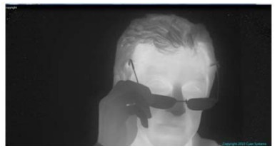
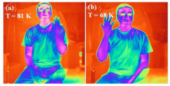
2010年,美国西北大学报道了二类超晶格长波红外焦平面探测器的研究进展[15]。为了抑制器件暗电流,他们采用了与中波相同的p-π-M-N结构,器件结构与能带排列如图 7所示[16]。77 K下,器件截止波长为11 μm,由于高的材料质量与厚的吸收区,器件的光响应很强,量子效率超过50%。M结构和双异质结设计同时降低体暗电流和表面漏电流。77 K工作温度和-50 mV工作电压下,器件的暗电流低于5×10⁻⁵ A/cm-2。利用此器件结构,西北大学验证了百万像素(1 k×1 k)规模的长波焦平面探测器,像元中心距18 μm。图 8给出了焦平面探测器在81 K和68 K下的成像照片[15],图像应用了两点非均匀性修正。另外,焦平面测试结果表明,在f/2与0.13 ms积分时间条件下,81 K时的NETD为27 mK,68 K时的19 mK。
![]() 图 7 p-π-M-N超晶格二极管的器件结构与能带图Figure 7. Device structure and band diagram of a p-π-M-N superlattice photodiode
图 7 p-π-M-N超晶格二极管的器件结构与能带图Figure 7. Device structure and band diagram of a p-π-M-N superlattice photodiode![]() 图 8 美国西北大学1 k×1 k长波焦平面在81 K和68 K拍摄的照片Figure 8. Image taken with the 1 k×1 k LWIR FPA of Northwestern University at 81 K and 68 K
图 8 美国西北大学1 k×1 k长波焦平面在81 K和68 K拍摄的照片Figure 8. Image taken with the 1 k×1 k LWIR FPA of Northwestern University at 81 K and 68 K同年,JPL也报道了InAs/GaSb二类超晶格长波红外焦平面探测器的研究进展[17]。JPL采用的CBIRD(complementary barrier infrared detector)器件结构,其能带排列如图 9所示。单元器件测试结果得到,80 K下,探测器截止波长为11.5 μm,量子效率32%。利用此CBIRD结构,JPL研制了1 k×1 k规模,像元中心距17.5 μm的焦平面探测器。焦平面测试结果得到量子效率为21%(与大面积单元测试结果基本吻合,因为焦平面填充因子为81%),在80 K工作温度、1 ms积分时间、f/2测试条件下,NETD为53 mK。80 K下的成像照片如图 10所示。
![]() 图 10 JPL InAs/GaSb超晶格长波红外焦平面拍摄的照片Figure 10. Image taken with the InAs/GaSb LWIR superlattice infrared FPA of JPL
图 10 JPL InAs/GaSb超晶格长波红外焦平面拍摄的照片Figure 10. Image taken with the InAs/GaSb LWIR superlattice infrared FPA of JPL2018年,JPL简短地报道了利用InAs/InAsSb超晶格作为吸收层的势垒型长波红外焦平面探测器的性能[18]。文中没有提到具体的器件结构,应该是与中波HOT-BIRD类似的nBn结构。在60 K工作温度下,探测器截止波长约为11.2 μm,量子效率约37%,暗电流约1×10⁻⁵ A/cm-2。并制备了640×512规格的焦平面探测器,在60 K工作温度,积分时间0.92 ms,f/4冷屏测试条件下,NETD为21 mK,有效像元率为99.7%,焦平面拍摄的照片如图 11所示。
![]() 图 11 JPL InAs/InAsSb超晶格长波红外焦平面探测器拍摄的照片Figure 11. Image taken with the InAs/InAsSb LWIR superlattice infrared FPA detector of JPL
图 11 JPL InAs/InAsSb超晶格长波红外焦平面探测器拍摄的照片Figure 11. Image taken with the InAs/InAsSb LWIR superlattice infrared FPA detector of JPL2015年,以色列SCD公司报道了其二类超晶格长波红外探测器的研究进展[19]。SCD采用的是pBp型器件结构,其中B是InAs/AlSb超晶格势垒层,其能带排列如图 12所示。利用pBp器件结构SCD制作了640×512规模,像元中心距15 μm的焦平面探测器(SCD称为Pelican-D LW)。焦平面测试结果得到,77 K下,器件截止波长9.5 μm,暗电流4.4×10⁻⁵ A/cm-2,量子效率约50%,NETD为15 mK(f/2.7,30 Hz),有效像元率大于99%。焦平面成像结果如图 13所示。
2.3 高性能双色焦平面
双色焦平面探测器可同时获取目标的两个红外波段的信息,以其装备的整机的探测与识别目标能力优于单波段同规格的热像仪。在恶劣天气、复杂背景或弱目标背景温差情况下,能较好地实现对目标的探测与识别,提高复杂背景下目前的探测效果与识别目前的能力,不容易受到干扰而引起混淆。可在侦查、预警、导弹防御和反导拦截等应用中发挥不可替代的作用,是红外焦平面技术最重要的发展方向之一。
德国AIM是最早报道InAs/GaSb二类超晶格双色焦平面探测器的研究机构。他们于2006年报道了中/中双色焦平面探测器[20],规模288×384,像元中心距40 μm。单元器件测试结果表明,77 K下,红色通道截止波长5 μm,蓝色通道截止波长4 μm;-50 mV常用偏压下的暗电流分别为,红色通道2.2×10⁻⁷ A/cm2,蓝色通道1.9×10-9 A/cm2。焦平面测试结果得到,蓝色通道NETD为29.5 mK,红色通道NETD为16.5 mK,其中测试条件为f/2冷屏、73 K工作温度、2.8 ms积分时间。2013年焦平面测试结果得到,蓝色通道NETD为14.6 mK,红色通道NETD为9.0 mK[21]。该中波双色焦平面探测器的成像效果如图 14[22]所示,其中青色代表“3.4~4 μm”波段的效果,红色代表“4~5 μm”波段的效果。利用两个波段成像效果的差异,可以区分出热二氧化碳和其它物体。因此该焦平面探测器可应用于导弹告警系统。
![]() 图 14 AIM 384×288中波双色二类超晶格焦平面成像效果Figure 14. Bispectral infrared image taken with 384×288 MWIR dual-band T2SL FPA of AIM
图 14 AIM 384×288中波双色二类超晶格焦平面成像效果Figure 14. Bispectral infrared image taken with 384×288 MWIR dual-band T2SL FPA of AIM美国西北大学基于他们在超晶格单色红外焦平面探测器的研究经验,很早便开始了超晶格双色红外焦平面探测器的研究,并于2012年报道了中长双色焦平面的研究[23]。单元器件测试结果表明,中波在160 K时,50%截止波长为5.2 μm,量子效率为40~50%,77 K时,R0A大约为106 Ω·cm2,探测率为7×10¹² Jones;长波在77 K时,50%截止波长为11.2 μm,量子效率超过30%(探测波长<9 μm时),R0A为600 Ω·cm2,探测率为2×10¹¹ Jones。焦平面(焦平面规模320×256)测试得到,中波NETD为10 mK,长波NETD为30 mK,测试条件为f/2和30 Hz,积分时间分别为10 ms和0.18 ms。焦平面成像照片如图 15所示。
![]() 图 15 美国西北大学320×256超晶格中长波双色焦平面拍摄的照片Figure 15. Imaging taken with 320×256 MWIR-LWIR dual-color T2SL FPA of Northwestern University
图 15 美国西北大学320×256超晶格中长波双色焦平面拍摄的照片Figure 15. Imaging taken with 320×256 MWIR-LWIR dual-color T2SL FPA of Northwestern University(a) MWIR (b) LWIR 在VISTA计划的支持下,休斯实验室也进行了超晶格中长双色焦平面探测器的研制,并在2017年报道了1280×720/12 μm超晶格中长双色焦平面探测器的研究进展[24]。文中未报道具体材料和器件结构,仅报道焦平面性能。80 K温度下,f/4.21测试条件,中波NETD为27.44 mK,3×平均NETD判据下的有效像元率为99.4%;长波NETD为27.62 mK,有效像元率为99.09%。焦平面成像演示照片如图 16所示。为了验证超晶格双色焦平面探测器制造技术的稳定性[25],2018年报道了在两年时间内制备的89个焦平面探测器的NETD有效像元率(3×平均NETD判据),如图 17所示,超过85%的焦平面探测器的双波段有效像元率大于99%。
![]() 图 16 休斯实验室中长双色焦平面探测器在80 K温度和f/4条件下拍摄的照片Figure 16. Pictures acquired with a MW/LW FPA of HRL at 80 K and f/4
图 16 休斯实验室中长双色焦平面探测器在80 K温度和f/4条件下拍摄的照片Figure 16. Pictures acquired with a MW/LW FPA of HRL at 80 K and f/4(a) MWIR (b) LWIR 为方便比较,表 1汇总了2005年至今不同公司不同波段超晶格红外焦平面探测器的性能参数。
表 1 不同探测波段探测器及焦平面性能参数Table 1. Performance parameter of detector and FPA under different detection regimeResearch Institute Device structure Operation temperature/K Cut-off wavelength/μm Quantum efficiency/% Dark current/A/cm-2 Detectivity/Jones FPA format/pitch NETD/mK Operability/% Publish year MWIR AIM n-i-p 77 5.4
(5% cutoff)30 256×256/40 μm 11.1 99.42 2005 Northwestern University p-π-M-N 150 4.2 1.05×10¹² 320×256 11.0@120 K 2011 HRL 150 5.0 50 without AR coating 6.3×10⁻⁶ 2 k×1 k/5 μm < 20@150 K, f/2.3, with subframe
averaging99.9 2017 JPL nBn 150 5.4 52 4.5×10⁻⁵ 640×512/24 μm 18.7 99.7 2018 LWIR Northwestern University p-π-M-N 77 11.0 >50 5.5×10⁻⁵ 1 k×1 k/18 μm 27 @81 K
19@68 K2010 JPL CBIRD 80 11.5 21 1 k×1 k/17.5 μm 53 2010 JPL nBn 60 11.2 37 1×10⁻⁵ 640×512 21 99.7% 2018 SCD pBp 77 9.5 ~50 4.4×10⁻⁵ 640×512/18 μm 15 (with 8 frame average) >99% 2016 Dual color IR AIM 77 4 (Blue)
5 (Red)2.2×10⁻⁷
1.9×10-7384×288/40 μm 29.5(Blue)
16.5 (Red)2006 Northwestern University 5.2 @160 K for MW
11.2
@77K for LW40-50@160K for MW
> 30
@77K for LW7.0×1012@160K for MW
2.0×10¹¹
@77K for LW320×256 10 (MW)
30 (LW)2012 HRL 80 1280×720/
12μm27.44 (MW)
27.62(LW)99.4(MW)
99.09(LW)2017 Note:Unless otherwise indicated, the cut-off wavelength refers to 50% cut-off wavelength 2.4 超晶格红外探测器的技术发展历程与未来发展方向
超晶格红外探测器近30年的发展历程如图 18所示。从技术发展角度看,超晶格红外探测器早期(2000年~2010年)主要采用传统p-i-n二极管结构。但是由于超晶格材料少子寿命(主要是Shockley-Read-Hall复合寿命,简称SRH寿命)较短,钝化难度较大,器件暗电流较高。随后在2010年前后,研究人员把目光转向势垒型探测器。势垒探测器是短SRH寿命材料更好的选择。相对于传统二极管结构,势垒型探测器结构有如下优势:①理论上,耗尽区产生复合电流可以被消除,可以很大程度上减低暗电流;②单级器件结构使钝化技术变得容易;③宽带隙势垒对位错的容忍度要高,使得红外材料可以生长在晶格失配的便宜的衬底上。因此,很多研究结构提出了不同的势垒探测器结构,这包括了西北大学提出的p-π-M-N结构[16],JPL提出的CBIRD结构[17],SCD公司的pBp结构等[19]。势垒的引入很大程度上抑制了暗电流,提高了器件性能。
![]() 图 18 二类超晶格红外探测器发展历程Figure 18. Roadmap of type-Ⅱ superlattice infrared photodetectors development
图 18 二类超晶格红外探测器发展历程Figure 18. Roadmap of type-Ⅱ superlattice infrared photodetectors development德国AIM公司和IAF研究所是比较早期开展超晶格红外焦平面探测器研制的机构。从2005年便开始报道中波红外焦平面探测器的研究结果,2006年又报道了中/中双色焦平面探测器的研究结果。其探测器结构采用的是传统p-i-n二极管结构。后续持续对这两款探测器进行优化改进。同时,也在开展超晶格长波红外探测器研制工作,但仅有器件结构设计和单元器件性能的报道,未见焦平面探测器结果。AIM公司的超晶格中/中双色红外焦平面探测器已经应用于欧洲大型运输机A400预警系统。
JPL作为美国VISTA计划重要参与者,在VISTA计划的支持下,不仅承担了器件结构设计与验证工作,还将其早年在材料生长积累的经验技术转移给IQE公司[16]。JPL从2007年开始报道其InAs/GaSb超晶格探测器材料生长的结果[26]。器件方面,从2009开始报道InAs/GaSb长波红外探测器结构设计和单元器件性能,为了抑制暗电流,提出了CIBRD结构[27],具体见图 9。并于2010年报道了基于CIBRD结构的长波红外焦平面探测器[17]。2010年~2016年期间,持续对其超晶格长波探测器结构(CBIRD)进行细节上的优化[28-31],以期提高器件性能。从2016年起开始对InAs/InAsSb超晶格探测器进行理论研究,认为InAs/InAsSb超晶格探测器在中波高温器件具有优势[32]。并在2018年报道了基于nBn结构的InAs/InAsSb超晶格中波高温焦平面探测器,工作温度达150 K。据报道,该探测器已应用于6U CubeSat卫星上的红外大气探测仪CIRAS(Cubesat Infrared Atmospheric Sounder)[33]。鉴于nBn型InAs/InAsSb超晶格在中波高温焦平面探测器上的成功,JPL将其应用于长波焦平面探测器,并在2018年进行过简短的报道,该探测器也应用于6U CubeSat卫星上的高光谱热像仪HyTI(Hyperspectral Thermal Imager)[26]。
由于休斯实验室在VISTA计划中承担的是红外焦平面探测器的研制工作,不进行器件结构设计和材料生长,因此仅有焦平面探测器性能相关的报道。HRL在2017年对超晶格中波高温焦平面探测器和中长双色焦平面探测进行了报道[12, 24]。HRL的中波高温焦平面探测器是目前为止报道的面阵规模最大,像元中心距最小的焦平面探测器,工作温度也达到150 K。HRL中长双色焦平面探测器研制报道也较为全面,证实了HRL在红焦平面探测器制备技术上的稳定性[25]。
美国西北大学是超晶格红外探测器研究起步比较早的研究机构。西北大学早期(2000年~2007年)的研究主要是超晶格材料生长[34],能带设计[35],以及传统p-i-n结构的单元器件和焦平面制备[36]。西北大学2007年提出P-π-M-N双异质结探测器结构。基于此结构在2011年和2010年分别研制了中波高温焦平面探测器[11]和长波焦平面探测器[15]。西北大学研究重点在开发出高性能的探测器结构,并进行焦平面验证,没有将精力放在后续结构优化和焦平面制备技术的改进。西北大学报道过包括短波、中波、长波、中短、中长、长长双色焦平面探测器的性能。后续在2014年将研究方向转到nBn型InAs/InAsSb超晶格上,报道过长波和甚长波探测器单元器件性能,但没有焦平面探测器的报道。
以色列SCD公司对超晶格探测器的研制中心主要放在长波红外探测器,以弥补其在长波碲镉汞探测器仅有288×4线列产品的不足。从2009年开始SCD对InAs/GaSb超晶格长波材料能带设计[37]、器件结构设计和单元器件性能进行了报道[38]。随后在2015年报道了基于pBp结构的长波焦平面探测器的性能[19],采用的是其提出的pBp势垒型探测器结构。2015年之后持续对其探测器结构和焦平面制备技术进行优化改进。SCD公司的Pelican-D LW长波红焦平面探测器是目前唯一的超晶格红外探测器货架产品。
从以上几家超晶格红外探测器领先的研究机构的研究历程来看,探测器的快速发展主要集中在2005年至今的16年间,相比于碲镉汞60年的研究历史,超晶格才刚刚起步不久,技术成熟相对较低。想要达到Grein等人[39]计算的极限暗电流性能(相较于碲镉汞rule07低两个量级),还需要在人力和物力方面进行较大的投资,在基础材料、器件结构设计和焦平面制备工艺技术方面有较大的突破,超晶格未来的研究重心还是在这3个方面。超晶格的未来发展方向主要在长波、甚长波,以及中长双色焦平面探测器的制备能力和性能提升上。
3. 国内二类超晶格材料与器件研究中存在的技术问题
理论预言二类超晶格具有比HgCdTe更好的性能,但是到目前为止,这些优越的性能还未完全实现。尽管如此,国外的超晶格红外探测器已经有货架产品和应用。但国内在二类超晶格红外探测器研制还有所不足,还未得到应用验证。不论在器件结构设计,材料生长还是器件制备技术上,仍然存在一些问题,仍有很多的研究工作要做。目前存在的问题总的来说有3个方面。
1)量子效率低,仅为30~50%,并没有达到预期。问题在于很难生长出具有足够厚度且质量不降低的材料,从而保证材料具有足够的吸收。
2)器件暗电流高。二类超晶格在暗电流工作温度下(77 K)主要由SRH产生复合电流主导,但SRH复合中心数量并没有得到很好地控制。虽然参考了国外各种新颖的势垒结构设计可以部分抑制SRH产生复合电流,但是针对器件结构具体参数设计和材料外延生长控制上,还有待改进。虽然当前器件暗电流有所改善,但相比于国外二类超晶格器件,以及国内外HgCdTe器件还存在一定的差距。
3)侧壁漏电流没有得到有效的抑制,特别是长波器件。在器件完成台面隔离后,超晶格材料在侧壁处突然终止,会形成大量的悬挂键。部分悬挂键将通过自然氧化被饱和,剩下的则在氧化物和半导体界面形成界面态,这些界面态将造成费米能级钉扎,在界面附近的半导体材料将产生能带弯曲,形成漏电通道,增加器件暗电流和噪声,降低器件性能,影响器件稳定性。因此需要通过侧壁钝化技术中和侧壁处超晶格材料突然终止形成的悬挂键,降低界面态密度,从而降低暗电流,提高器件的性能。虽然目前对表面钝化技术进行了大量的研究工作,取得了一定的进展,但是何种钝化技术更为有效、稳定并没有达成共识。器件性能的进一步提高还有待于钝化技术的改进。
4. 小结
本文简要介绍了二类超晶格用于红外探测器的优势,总结了国际上二类超晶格红外探测器研究领域较为领先的研究机构(包括美国的西北大学量子器件中心、喷气推进实验室、休斯实验室,德国弗朗霍夫协会应用固体物理研究所和AIM公司,以色列的SCD公司)在二类超晶格红外探测器研制中的进展与技术发展历程,并对国内在二类超晶格红外探测器研究中存在地问题进行了分析。
-
![]()
图 2 AIM InAs/GaSb超晶格中波二极管截面示意图
Figure 2. Schematic cross section of an InAs/GaSb SL MWIR diode of AIM
![]()
图 3 AIM InAs/GaSb超晶格256×256中波焦平面成像系统拍摄的照片
Figure 3. Thermal images taken with the InAs/GaSb superlattice 256×256 MWIR FPA camera system of AIM
![]()
图 4 美国西北大学中波焦平面探测器在120 K(a)和150 K(b)下的成像照片,(c) 86-150 K下焦平面的NTED
Figure 4. Images taken with a MWIR FPA detector of Northwestern University operating at (a) 120 K and (b) 150 K (c) NEDT measured from 86 to150 K
![]()
图 5 休斯实验室1 k×2 k/5 μm焦平面在150 K下拍摄的照片
Figure 5. Image captured by a 1 k×2 k/5 μm MWIR FPA of HRL operated at 150 K
![]()
图 6 JPL 640×512规格InAs/InAsSb超晶格中波红外焦平面拍摄的照片
Figure 6. Images taken at 160 K and 170 K using a 640×512 format InAs/InAsSb superlattice MWIR focal plane array of JPL
![]()
图 7 p-π-M-N超晶格二极管的器件结构与能带图
Figure 7. Device structure and band diagram of a p-π-M-N superlattice photodiode
![]()
图 8 美国西北大学1 k×1 k长波焦平面在81 K和68 K拍摄的照片
Figure 8. Image taken with the 1 k×1 k LWIR FPA of Northwestern University at 81 K and 68 K
![]()
图 10 JPL InAs/GaSb超晶格长波红外焦平面拍摄的照片
Figure 10. Image taken with the InAs/GaSb LWIR superlattice infrared FPA of JPL
![]()
图 11 JPL InAs/InAsSb超晶格长波红外焦平面探测器拍摄的照片
Figure 11. Image taken with the InAs/InAsSb LWIR superlattice infrared FPA detector of JPL
![]()
图 14 AIM 384×288中波双色二类超晶格焦平面成像效果
Figure 14. Bispectral infrared image taken with 384×288 MWIR dual-band T2SL FPA of AIM
![]()
图 15 美国西北大学320×256超晶格中长波双色焦平面拍摄的照片
Figure 15. Imaging taken with 320×256 MWIR-LWIR dual-color T2SL FPA of Northwestern University
(a) MWIR (b) LWIR ![]()
图 16 休斯实验室中长双色焦平面探测器在80 K温度和f/4条件下拍摄的照片
Figure 16. Pictures acquired with a MW/LW FPA of HRL at 80 K and f/4
(a) MWIR (b) LWIR ![]()
图 18 二类超晶格红外探测器发展历程
Figure 18. Roadmap of type-Ⅱ superlattice infrared photodetectors development
表 1 不同探测波段探测器及焦平面性能参数
Table 1 Performance parameter of detector and FPA under different detection regime
Research Institute Device structure Operation temperature/K Cut-off wavelength/μm Quantum efficiency/% Dark current/A/cm-2 Detectivity/Jones FPA format/pitch NETD/mK Operability/% Publish year MWIR AIM n-i-p 77 5.4
(5% cutoff)30 256×256/40 μm 11.1 99.42 2005 Northwestern University p-π-M-N 150 4.2 1.05×10¹² 320×256 11.0@120 K 2011 HRL 150 5.0 50 without AR coating 6.3×10⁻⁶ 2 k×1 k/5 μm < 20@150 K, f/2.3, with subframe
averaging99.9 2017 JPL nBn 150 5.4 52 4.5×10⁻⁵ 640×512/24 μm 18.7 99.7 2018 LWIR Northwestern University p-π-M-N 77 11.0 >50 5.5×10⁻⁵ 1 k×1 k/18 μm 27 @81 K
19@68 K2010 JPL CBIRD 80 11.5 21 1 k×1 k/17.5 μm 53 2010 JPL nBn 60 11.2 37 1×10⁻⁵ 640×512 21 99.7% 2018 SCD pBp 77 9.5 ~50 4.4×10⁻⁵ 640×512/18 μm 15 (with 8 frame average) >99% 2016 Dual color IR AIM 77 4 (Blue)
5 (Red)2.2×10⁻⁷
1.9×10-7384×288/40 μm 29.5(Blue)
16.5 (Red)2006 Northwestern University 5.2 @160 K for MW
11.2
@77K for LW40-50@160K for MW
> 30
@77K for LW7.0×1012@160K for MW
2.0×10¹¹
@77K for LW320×256 10 (MW)
30 (LW)2012 HRL 80 1280×720/
12μm27.44 (MW)
27.62(LW)99.4(MW)
99.09(LW)2017 Note:Unless otherwise indicated, the cut-off wavelength refers to 50% cut-off wavelength  下载: 导出CSV
-
[1] Sai-halasz G A, Tsu R, Esaki L. A new semiconductor superlattice[J]. Appl. Phys. Lett., 1977, 30: 651. DOI: 10.1063/1.89273
[2] Sai-halasz G A, Esaki L, Harrison W A. InAs/GaSb superlattice energy structure and its semiconductor-semimetal transition[J]. Phys. Rev. B, 1978, 18: 2812. DOI: 10.1103/PhysRevB.18.2812
[3] Smith D L, Mailhiot C. Proposal for strained type Ⅱ superlattice infrared detectors[J]. J. Appl. Phys., 1987, 62: 2545. DOI: 10.1063/1.339468
[4] Johnson J L, Samoska L A, Gossard A C, et al. Electrical and optical properties of infrared photodiodes using the InAs/Ga1−xInxSb superlattice in heterojunctions with GaSb[J]. J. Appl. Phys., 1996, 80: 1116. DOI: 10.1063/1.362849
[5] Rogalski A, Kopytko M, Martyniuk P. InAs/GaSb type-Ⅱ superlattice infrared detectors: three decades of development[C]//Proc. of SPIE, 2017, 10117: 1017715.
[6] Plis E A, InAs/GaSb type-Ⅱ superlattice detectors[J]. Adv. Electron., 2014, 2014: 246769
[7] 尚林涛, 王静, 邢伟荣, 等. 红外探测Ⅱ类超晶格技术概述(一)[J]. 激光与红外, 2021, 51(4): 404. DOI: 10.3969/j.issn.1001-5078.2021.04.002 [8] 尚林涛, 王静, 邢伟荣, 等. 红外探测Ⅱ类超晶格技术概述(二)[J]. 激光与红外, 2021, 51(5): 548. DOI: 10.3969/j.issn.1001-5078.2021.05.002 [9] Walther M, Rehm R, Fuchs F, et al, 256×256 Focal Plane Array Midwavelength Infrared Camera Based on InAs/GaSb Short-Period Superlattices[J]. J. Electron. Mater., 2005, 34: 722. DOI: 10.1007/s11664-005-0010-z
[10] Rehm R, Walther M, Schmitz J, et al. 2nd and 3rd Generation Thermal Imagers based on Type-Ⅱ Superlattice Photodiodes[C]//Proc. of SPIE, 2006, 6294: 629404.
[11] Pour S A, HUANG E K, CHEN G, et al. High operating temperature midwave infrared photodiodes and focal plane arrays based on type-Ⅱ InAs/GaSb superlattices[J]. Appl. Phys. Lett., 2011, 98: 143501. DOI: 10.1063/1.3573867
[12] Sharifi H, Roebuck M, Terterian S, et al. Advances in Ⅲ-Ⅴ Bulk and Superlattice-based High Operating Temperature MWIR Detector Technology[C]//Proc. of SPIE, 2017, 10177: 101770U.
[13] TING D Z, Soibel A, Khoshakhlagh A, et al. Mid-w avelength high operating temperature barrier infrared detector and focal plane arrays[J]. Appl. Phys. Lett., 2018, 113: 021101. DOI: 10.1063/1.5033338
[14] Ting D Z, Soibel A, Khoshakhlagh A, et al. Antimonide type-Ⅱ superlattice barrier infrared detectors[C]//Proc. of SPIE, 2018, 10177: 101770N.
[15] Manurkar P, Ramezani-Darvish S, Nguyen B M, et al. High performance long wavelength infrared mega-pixel focal plane array based on type-Ⅱ superlattices[J]. Appl. Phys. Lett., 2010, 97: 193505. DOI: 10.1063/1.3514244
[16] Razeghi M, Haddadi A, Hoang A M, et al. Antimonide-Based Type Ⅱ Superlattices: A Superior Candidate for the Third Generation of Infrared Imaging Systems[J]. J. Electron. Mater., 2014, 43: 2802-2807. DOI: 10.1007/s11664-014-3080-y
[17] Gunapala S D, Ting D Z, Hill C J, et al. Demonstration of a 1024×1024 Pixel InAs-GaSb Superlattice Focal Plane Array[J]. IEEE Photonic Tech. Lett., 2010, 22: 1856. DOI: 10.1109/LPT.2010.2089677
[18] Ting D Z, Soibel A, Khoshakhlagh A, et al. Antimonide e-SWIR, MWIR, and LWIR barrier infrared detector and focal plane array development[C]//Proc. of SPIE, 2018, 10624: 1062410.
[19] Klipstein P C, Avnon E, Benny Y, et al. Type-Ⅱ superlattice detector for long-wave infrared imaging[C]//Proc. of SPIE, 2015, 9451: 94510K.
[20] Rehm R, Walther M, Schmitz J, et al. Dual-colour thermal imaging with InAs/GaSb superlattices in mid-wavelength infrared spectral range[J]. Electron. Lett., 2006, 42: 577. DOI: 10.1049/el:20060878
[21] Wörl A, Rutz F, Rehm R, et al. Electro-Optical Properties of InAs/GaSb Superlattice Infrared Photodiodes for Bispectral Detection[C]//Proceedings IRS, 2013: 37-42.
[22] Rutz F, Walther M, Schmitz J, et al. InAs/GaSb superlattices for advanced infrared focal plane arrays[J]. Infrared Phys. Techn., 2009, 52: 344. DOI: 10.1016/j.infrared.2009.09.005
[23] HUANG E K, HOANG M A, CHEN G, et al. Highly selective two-color mid-wave and long-wave infrared detector hybrid based on Type-Ⅱ superlattices[J]. Opt. Lett., 2012, 37: 4744. DOI: 10.1364/OL.37.004744
[24] Delaunay P Y, Nosho B Z, Gurga A R, et al. Advances in Ⅲ-Ⅴ Based Dual-Band MWIR/LWIR FPAs at HRL[C]//Proc. of SPIE, 2017, 10177: 101770T.
[25] Gurga A R, Nosho B Z, Terterian S, et al. Dual-Band MWIR/LWIR Focal Plane Arrays based on Ⅲ-Ⅴ Strained-Layer Superlattices[C]//Proc. of SPIE, 2018, 10624: 106240O.
[26] Hill C J, Li J V, Mumolo J M, Gunapala S D, MBE grown type-Ⅱ MWIR and LWIR superlattice photodiodes[J]. Infrared Phys. Techn., 2007, 50: 187. DOI: 10.1016/j.infrared.2006.10.033
[27] Ting D Z, Hill C J, Soibel A, et al. A high-performance long wavelength superlattice complementary barrier infrared detector[J]. Appl. Phys. Lett., 2009, 95: 023508. DOI: 10.1063/1.3177333
[28] Soibel A, Nguyen J, Höglund L, et al. InAs/GaSb superlattice based long-wavelength infrared detectors: Growth, processing, and characterization[J]. Infrared Phys. Techn., 2011, 54: 247. DOI: 10.1016/j.infrared.2010.12.023
[29] Höglund L, Soibel A, Ting D Z, et al. Minority carrier lifetime and photoluminescence studies of antimony based superlattices[C]//Proc. of SPIE, 2012, 8511: 851106.
[30] Ting D Z, Soibel A, Khoshakhlagh A, et al. Complementary barrier infrared detector (CBIRD) with double tunnel junction contact and quantum dot barrier infrared detector (QD-BIRD)[J]. Infrared Phys. Techn., 2013, 59: 146. DOI: 10.1016/j.infrared.2012.12.030
[31] Ting D Z, Soibel A, Gunapala S D, Hole effective masses and subband splitting in type-Ⅱ superlattice infrared detectors[J]. Appl. Phys. Lett., 2016, 108: 183504. DOI: 10.1063/1.4948387
[32] Ting D Z, Soibel A, Khoshakhlagh A, et al. Antimonide type-Ⅱ superlattice barrier infrared detectors[C]//Proc. of SPIE, 2017, 10177: 101770N.
[33] Gunapala S D, TING D Z, Rafol S, et al. Antimonides T2SL Mid-Wave and Long-Wave Infrared Focal Plane Arrays for Earth Remote Sensing Applications[C]//Proc. of SPIE, 2020, 11288: 112880K.
[34] Wei Y, Gin A, Razeghi M, et al. Type Ⅱ InAs/GaSb superlattice photovoltaic detectors with cutoff wavelength approaching 32 μm[J]. Appl. Phys. Lett., 2002, 81: 3675. DOI: 10.1063/1.1520699
[35] Nguyen B-M., Razeghi M, Nathan V, et al. Type-Ⅱ "M" Structure Photodiodes: An Alternative Material Design for Mid-Wave to Long Wavelength Infrared Regimes[C]//Proc. of SPIE, 2007, 6479: 64790S.
[36] Delaunay P-Y, Nguyen B M, Hoffman D, et al. 320×256 infrared Focal Plane Array based on Type Ⅱ InAs/GaSb superlattice with a 12 µm cutoff wavelength[C]//Proc. of SPIE, 2007, 6542: 654204.
[37] Livneh Y, Klipstein P C, Klin O, et al. k·p model for the energy dispersions and absorption spectra of InAs/GaSb type-Ⅱ superlattices[J]. Phys. Rev. B, 2012, 86, 235311. DOI: 10.1103/PhysRevB.86.235311
[38] Klipstein P C, Avnon E, Benny Y, et al. InAs/GaSb Type Ⅱ superlattice barrier devices with a low dark current and a high quantum efficiency. [C]//Proc. of SPIE, 2014, 9070: 90700U.
[39] Grein C H, Garland J, Flatte M E. Strained and unstrained layer superlattices for infrared detection[J]. J. Electron. Mater., 2009, 38: 1800. DOI: 10.1007/s11664-009-0757-8
-
期刊类型引用(3)
1. 李景峰,刘铭,李海燕,温涛,赵成城,王丹. 低损伤、高深宽比Ⅱ类超晶格材料的台面刻蚀技术研究. 红外. 2023(03): 1-7 .  百度学术
百度学术
2. 潘晓凯,姜梦杰,王东,吕旭阳,蓝诗琪,卫英东,何源,郭书广,陈平平,王林,陈效双,陆卫. 红外-太赫兹光电探测器应用及前沿变革趋势. 量子电子学报. 2023(02): 217-237 . 百度学术
3. 严定钰,沈祥,王庶民,石张勇,张焱超,张凡. AlAsSb的外延再生长对InAs/GaSb红外探测器暗电流抑制效果研究. 宁波大学学报(理工版). 2023(03): 87-93 . 百度学术
其他类型引用(5)


计量
- 文章访问数: 650
- HTML全文浏览量: 68
- PDF下载量: 282
- 被引次数: 8
