

Research Progress in the Metal Oxide Heterojunction Photodetectors
-
摘要: 金属氧化物(metal oxide,MO)因其具有易于制备、高稳定性、对载流子的选择性传输等优点,被广泛应用于光电探测领域。MO材料具有较强的光吸收,但表面效应和缺陷态等问题导致了MO光电探测器响应速度低和暗电流较大的问题。异质结中的内建电场可以有效促进光生电子-空穴对的分离,从而提升器件响应速度和降低器件暗电流。因此,构建金属氧化物异质结光电探测器(heterojunction photodetectors,HPDs),对于MO在光电子领域的进一步应用具有重要的意义。本文先介绍了MO的界面性质,然后围绕PN、PIN和同型异质结3种结构,对金属氧化物HPDs的工作机制进行了阐述。接着对响应波段在紫外-可见-近红外光区的、具有不同结构的MO/MO和MO/Si HPDs的性能参数进行了分析和比较,并讨论了金属氧化物HPDs的性能优化方法,最后对金属氧化物HPDs的发展进行了展望。Abstract: Metal oxides (MOs) have been widely used in photodetection because of advantages such as easy preparation, high stability, and selective transport of carriers. The MO materials exhibit strong light absorption properties. However, there are issues with MO photodetectors such as their low response speed and large dark current owing to the surface effects and defect states. The built-in electric field in the heterojunction can effectively promote the separation of photogenerated electron-hole pairs, thus improving the device response speed and reducing the dark current. Thus, the construction of metal oxide heterojunction photodetectors (HPDs) is of great significance for the further application of MO in the field of optoelectronics. This paper introduces the interface properties of MO and elaborates on the working mechanism of metal oxide HPDs around the PN, PIN, and isotype heterojunctions. Next, the performance parameters of MO/MO and MO/Si HPDs with different structure and response in UV-Vis-NIR band are analyzed and compared. Subsequently, improved methods of the metal oxide HPDs performances are discussed. Finally, the development of metal oxide HPDs is discussed.
-
Key words:
- photodetector /
- metal oxide /
- silicon /
- heterojunction
-

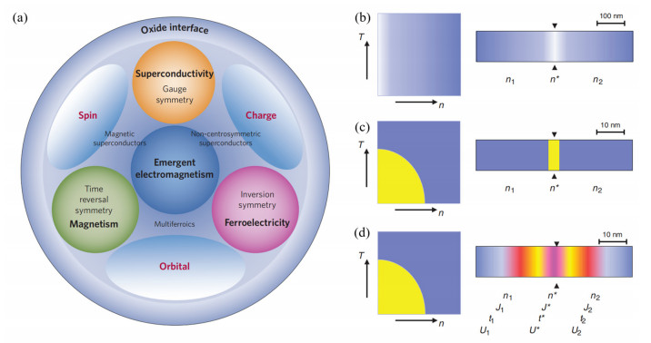
图 2 MO的界面特性:(a) 在MO界面上可以设计的关联电子的对称性和自由度[12];(b) 传统半导体的相图(左)和界面电子行为(右);(c)和(d)MO的相图(左)和界面电子行为(右),分别对应于产生电子形变(c)和不产生电子形变的情形(d)[13]
Figure 2. Properties of the MO interfaces: (a) The symmetries and degrees of freedom of correlated electrons that can be engineered at MO interfaces[12]; (b) Phase diagrams (left) and interface electronic behaviors (right) for conventional semiconductors; (c) and (d) Phase diagrams (left) and interface electronic behaviors (right) for MO, corresponding to the situations in which (c) and no electronic deformation is generated (d), respectively[13]

图 3 金属氧化物HPDs的载流子传输机制:(a) MO/MO和(b)MO/Si PN结HPDs的能带示意图[23-24];(c) MO/MO和(d) MO/Si PIN结HPDs能带示意图[25-26];(e) MO/MO和(f) MO/Si同型异质结HPDs能带示意图[27-28]
Figure 3. Carrier transport mechanism of metal oxide HPDs: The energy band diagrams of (a) MO/MO and (b) MO/Si PN junction HPDs[23-24]; (c) MO/MO and (d) MO/Si PIN junction HPDs[25-26]; (e) MO/MO and (f) MO/Si isotype HPDs[27-28]

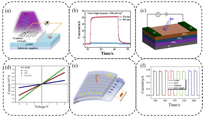
图 5 薄膜型MO/MO HPDs的结构和性能:(a) n-Ga2O3/p-NiO HPD的结构[71];(b) n-Ga2O3/p-NiO HPD的瞬态响应行为[71];(c) WO3/TiO2 HPD的结构[28];(d) TiO2,WO3和WO3/TiO2 PD I-V特性[28];(e) 柔性ZnO/SrCoOx HPD的结构[40];(f) ZnO/SrCoOx HPD在不同弯曲状态下的I-T曲线[40]
Figure 5. Structures and properties of the film-based MO/MO HPDs: (a) The structure of n-Ga2O3/p-NiO HPD[71]; (b) Transient response behavior of n-Ga2O3/p-NiO HPD[71]; (c) The structure of the WO3/TiO2 HPD[28]; (d) I-V characteristic of TiO2, WO3 and WO3/TiO2 PD[28]; (e) The structure of the flexible ZnO/SrCoOx HPD[40]; (f) I-T curves of the ZnO/SrCoOx HPD in different bending states[40]

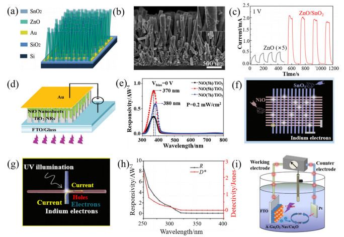
图 6 其他结构的MO/MO HPDs的性能:(a) ZnO/SnO2核壳纳米棒阵列HPD的结构[61];(b) ZnO/SnO2核壳纳米棒阵列的横截面SEM图像[61];(c) ZnO/SnO2 HPD在1 V偏压下的I-T曲线[61];(d) NiO纳米片/ZnO纳米棒阵列HPD的结构[73];(e) 零偏下的响应率在300~800 nm波长范围内的变化[73];(f) 横杆NiO/SnO2纳米纤维阵列HPD的结构[35];(g) NiO/SnO2 HPD的工作原理[35];(h) NiO/SnO2HPD在-5 V偏压下的响应率和探测率曲线[35];(i) α‑Ga2O3纳米棒阵列/Cu2O纳米球HPD的结构及其测试系统[39]
Figure 6. Properties of MO/MO HPDs with other structures: (a) The structure of ZnO/SnO2 core-shell nanorods array HPD[61]; (b) Cross-sectional SEM images of ZnO/SnO2 core-shell nanorods array[61]; (c) I-T curves of ZnO/SnO2 HPD at 1V bias[61]; (d) Structure of NiO nanosheet/ZnO nanorods array HPD[73]; (e) Wavelength-dependent responsivity at zero bias ranging from 300-800 nm[73]; (f) Structure of cross-bar NiO/SnO2 nanofiber array HPD[35]; (g) Working principle of the NiO/SnO2 HPD[35]; (h) Responsivity and detectivity curves of NiO/SnO2 HPD at -5 V bias[35]; (i) Structure and testing system of α‑Ga2O3 nanorods array/Cu2O nanosphere HPD[39]

图 7 MO/Si HPDs的结构和性能:(a) p-NiO/n-Si HPD的结构[76];(b) p-NiO/n-Si HPD I-V特性,插图显示了I-V曲线的局部放大图[76];(c) n-ZnO纳米管/p-Si HPD的结构[55];(d) n-ZnO/p-Si HPD的响应率和探测率曲线[55];(e) r-GO/n-Si HPD的结构[51];(f) r-GO/n-Si HPD的瞬态响应[51]
Figure 7. Structures and properties of MO/Si HPDs: (a) Structure of p-NiO/n-Si HPD[76]; (b) I-V characteristic curves of the p-NiO/n-Si HPD, the inset shows a close-up view of the I-V curves[76]; (c) Structure of the n-ZnO nanotubes/p-Si HPD[55]; (d) The responsivity and detectivity curves of the n-ZnO/p-Si HPD[55]; (e) Structure of the r-GO/n-Si HPD[51]; (f)Transient response of the r-GO/n-Si HPD[51]

图 8 金属氧化物HPDs的性能优化:(a) ε-Ga2O3/p-Si和ε-Ga2O3/Al2O3/p-Si HPDs的log I-V曲线[26];(b) NiO/ZnO和NiO/TiO2/ZnO HPDs在暗条件的log I-V曲线[67];(c) MoO3-x/Si HPD在光照下的J−V曲线[48];(d) p-NiO/n-ZnO和Pd NPs/p-NiO/n-ZnO NWs在可调制紫外光下的光电流和暗电流比[84];(e) Pd NPs/p-NiO/n-ZnO NWs的能带图[84];(f) 采用Al六方点等离子体阵列制备的Pd/TiO2/p-Si/Al HPD[87];(g) NiOx/n-Si和p-Ag: NiOx/n-Si HPDs的响应光谱[88];(h) 不同Eu掺杂浓度的TiO2薄膜的Tauc图[89];(i) n-β-Ga2O3/p-MnO QD和n-β-Ga2O3器件的响应光谱[37]
Figure 8. Performance optimization of metal oxide HPDs (a) Log I-V curves of ε-Ga2O3/p-Si and ε-Ga2O3/Al2O3/p-Si HPDs[26]; (b) Log I-V curves of NiO/ZnO and NiO/TiO2/ZnO HPDs in the dark[67]; (c) J-V curves of MoO3−x/Si HPD under illumination[48]; (d) Iphoto/Idark ratios for the p-NiO/n-ZnO and Pd NPs/p-NiO/n-ZnO NWs unde modulated UV illumination[84]; (e) Band diagrams for Pd NPs/p-NiO/n-ZnO NWs[84]; (f) Design of the fabricated Pd/TiO2/p-Si/Al HPD with Al hexagonal dots plasmonic array[87]; (g) Response spectra of NiOx/n-Si and p-Ag: NiOx/n-Si HPDs[88]; (h) Tauc plots of Eu: TiO2 films with different doping concentration[89]; (i) Response spectra of n-β-Ga2O3/p-MnO QDs and n-β-Ga2O3 device[37]
表 1 不同MOs的性质
Table 1. Properties of different MOs
MOs Conduction type Eg/(eV) Exciton binding energy/(meV) Crystal system Space group Ref. ZnO(Wurtzite) n 3.3 60 Hexagonal P63mc [2] TiO2(Anatase) n 3.2 130 Tetragonal C4/amc [3] TiO2(Rutile) n 3.0 130 Tetragonal P42/mmm [3] β-Ga2O3 n 4.9 40-50 Monoclinic C2/m [4] SnO2 n 3.6 130 Tetragonal P42/mnm [5] MoO3 p 3.0 - Orthorhombic - [6] V2O5 P 2.3 - Monoclinic P21/C [7] NiO P 3.6 110 Cubic Fm3m [8]  下载: 导出CSV
表 2 MO/MO和MO/Si HPDs的性能参数对比
Table 2. Comparisons of performance parameters for MO/MO and MO/Si HPDs
Year Structure Fabrication method Bias/V λ/nm EQE/(%) R/(AW−1) D*/Jones Rectification ratio Rise/fall time Ref. 2012 α-Fe2O3/p-Si Chemical solution deposition - 403 - 2×10³ - - < 1 ms [43] 2012 TiO2/SrTiO3 Sol-gel 10 260 - 46.1 - - 3.5 ms/1.4 s [44] 2014 NiO/ZnO Spin coating -1 350 1800 10.2 4.66×10¹² 5×10² - [45] 2015 CuO/SnO2 Magnetron sputtering 0.2 290 - 10.3 - - - [46] 2015 MgZnO/i-MgO/p-Si MOCVD 6 240 600 1.16 - - 15 μs [47] 2015 MoO3−x/n-Si Thermal evaporation 0 900 - - 6.29×10¹² - 1/51.4 μs [48] 2016 β-Ga2O3/p-Si Pulsed laser deposition 3 254 1.8×10⁵ 370 - - 1.79/0.27 s [49] 2016 Mg0.18Zn0.82O/p-Si Magnetron sputtering - 320 - 4.21 - 32500 - [50] 2016 GO/n-Si Modified Hummers method - 600 - 1.52 - - 2/3.7 ms [51] 2017 NiO/n-Si Magnetron sputtering 5 365 - 4.5 - - 266/200 ms [52] 2017 SnO2/SiO2/p-Si Magnetron sputtering -1 365 - 0.355 2.66×10¹² - < 0.1 s [53] 2017 TiO2/NiO Sol-gel
spin-coating and oxidation6 280 80500 181.9 1.56×10¹⁴ - 717/598 ms [54] 2017 p-Si/n-ZnO NTs Pulsed laser deposition -5 365 - 101.2 - - 0.44/0.59 s [55] 2019 n-TiO2/p-Si Thermal oxidation -4 365 - 6.74 1.31×10¹² - 127.6 /120.3 μs [56] 2019 V2O5/n-Si Thermal evaporation - 940 - 0.185 1.34×10¹² - 9.5/123 μs [57] 2019 ZnO/NiO Electrospinning 0 350 - 0.415×10⁻³ - - 7.5/4.8 s [58] 2019 n-SnO2/SiNWs Metal assisted chemical etching 5 UV - 0.35 8.03×10¹² 172.3 - [59] 2020 NiO/β-Ga2O3 Magnetron sputtering 10 245 - 27.43 3.14×10¹² - - [60] 2020 ZnO/SnO2 core-shell NAs Chemical liquid deposition 1 365 - 28.5(± 0.6) 2.9× 10¹⁴ - 8.7 s/20.8 s [61] 2020 p-Cu2O/n-Si Successive ionic layer
adsorption and reaction-5 500 3780 16.2 1.78×10¹²(−0.1 V) 118.4 < 10 ms [62] 2021 MoO3−x/Al2O3/n-Si Thermal evaporation -5 980 900 7.11 9.85×10¹² - 0.109/0.69 ms [63] 2022 NiO/IGZO Magnetron sputtering 0 365 - 0.0288 6.99×10¹¹ 7.4×10⁴ 15/31 ms [64] 2022 p-Mn2O3/n-Si Rapid thermal
oxidation- 500 140 0.5 7.2×10¹² - - [65] 2022 p-Ag2O/n-Si Rapid thermal
oxidation-4 450 118 0.43 9×10¹¹ - - [66] 2023 NiO/TiO2/ZnO Magnetron sputtering 2 365 - 291 6.9×10¹¹ 104 163/282 ms [67] 2023 p-NiO/SiO2/n-ZnO Magnetron sputtering 2 365 2×10³ 5.77 1.51×10¹¹ 57 48 ms [68] 2023 p-NiO/n-ZnO/n-Si Magnetron sputtering -1 280 - 3.672 3.3×10¹² - 10.5/0.4 s [69]
下载: 导出CSV
-
[1] YU X, Marks T J, Facchetti A. Metal oxides for optoelectronic applications[J]. Nature Materials, 2016, 15(4): 383-396. doi: 10.1038/nmat4599 [2] YAO J Q, DENG H, LI M, et al. Improving processes on ZnO-based ultraviolet photodetector[J]. Advanced Materials Research, 2013, 685: 195-200. doi: 10.4028/www.scientific.net/AMR.685.195 [3] Goldberg Y. Semiconductor near-ultraviolet photoelectronics[J]. Semiconductor Technology, 1999, 14(7): R41. doi: 10.1088/0268-1242/14/7/201 [4] CHEN X, REN F, GU S, et al. Review of gallium-oxide-based solar -blind ultraviolet photodetectors[J]. Photonics Research, 2019, 7(4): 381-415. doi: 10.1364/PRJ.7.000381 [5] Kar A, Stroscio M A, Dutta M, et al. Meyyappan, Observation of ultraviolet emission and effect of surface states on the luminescence from tin oxide nanowires[J]. Applied Physics Letters, 2009, 94: 101905. doi: 10.1063/1.3097011 [6] LI Lin, SUN Yuxuan, SUN Weifeng. First-principles study of electronic structure, magnetic and optical properties of laminated molybdenum oxides[J]. Acta PhysicaSinica, 2019, 68(5): 057101-3. [7] XIAO Z R, GUO G Y. Structural, electronic and magnetic properties of V2O5-x: An ab initio study[J]. The Journal of Chemical Physics, 2009, 130(21): 214704. doi: 10.1063/1.3146790 [8] Hwang J D, Chen H Y, Chen Y H, et al. Effect of nickel diffusion and oxygen behavior on heterojunction Schottky diodes of Au/NiO/ZnO with a NiO interlayer prepared by radio-frequency magnetron sputtering[J]. Nanotechnology, 2018, 29(29): 295705. doi: 10.1088/1361-6528/aac230 [9] OUYANG W, TENG F, HE J H, et al. Enhancing the photoelectric performance of photodetectors based on metal oxide semiconductors by charge-carrier engineering[J]. Advanced Functional Materials, 2019, 29(9): 1807672. doi: 10.1002/adfm.201807672 [10] 郭天超. 金属氧化物/硅异质结光电探测器的构建及性能调控[D]. 北京: 中国石油大学, 2020: 16.GUO Tianchao, Construction and Performance Modulation of Metal Oxides/Silicon Heterojunction Photodetectors[D]. Beijing: China University of Petroleum, 2020: 16. [11] CHEN S, FU Y, Ishaq M, et al. Carrier recombination suppression and transport enhancement enable high-performance self-powered broadband Sb2Se3 photodetectors[J]. InfoMat, 2023, 5(4): e12400. doi: 10.1002/inf2.12400 [12] HWANG H Y, Iwasa Y, Kawasaki M, et al. Emergent phenomena at oxide interfaces[J]. Nature Materials, 2012, 11(2): 103-113. doi: 10.1038/nmat3223 [13] Mannhart J, Schlom D G. Oxide interfaces—an opportunity for electronics[J]. Science, 2010, 327(5973): 1607-1611. doi: 10.1126/science.1181862 [14] Kennedy D. Breakthrough of the year[J]. Science, 2007, 318(5858): 1833-1833. doi: 10.1126/science.1154158 [15] Shim M, Guyot-Sionnest P. N-type colloidal semiconductor nanocrystals[J]. Nature, 2000, 407(6807): 981-983. doi: 10.1038/35039577 [16] JI T, LIU Q, ZOU R, et al. Enhanced UV-visible light photodetectors with a TiO2/Si heterojunction using band engineering[J]. Journal of Materials Chemistry C, 2017, 5(48): 12848-12856. doi: 10.1039/C7TC04811D [17] CHEN X, XU Y, ZHOU D, et al. Solar-blind photodetector with high avalanche gains and bias-tunable detecting functionality based on metastable phase α-Ga2O3/ZnO isotype heterostructures[J]. ACS Applied materials & Interfaces, 2017, 9(42): 36997-37005. [18] Serin N, Yildiz A, Alsaç A A, et al. Estimation of compensation ratio by identifying the presence of different hopping conduction mechanisms in SnO2 thin films[J]. Thin Solid Films, 2011, 519(7): 2302-2307. doi: 10.1016/j.tsf.2010.11.027 [19] Choi J M, Im S. Ultraviolet enhanced Si-photodetector using p-NiO films[J]. Applied Surface Science, 2005, 244(1-4): 435-438. doi: 10.1016/j.apsusc.2004.09.152 [20] Almora O, Gerling L G, Voz C, et al. Superior performance of V2O5 as hole selective contact over other transition metal oxides in silicon heterojunction solar cells[J]. Solar Energy Materials and Solar Cells, 2017, 168: 221-226. doi: 10.1016/j.solmat.2017.04.042 [21] Bullock J, WAN Y, XU Z, et al. Stable dopant-free asymmetric heterocontact silicon solar cells with efficiencies above 20%[J]. ACS Energy Letters, 2018, 3(3): 508-513. doi: 10.1021/acsenergylett.7b01279 [22] WU W, BAO J, JIA X, et al. Dopant-free back contact silicon heterojunction solar cells employing transition metal oxide emitters[J]. PhysicaStatus Solidi-Rapid Research Letters, 2016, 10(9): 662-667. doi: 10.1002/pssr.201600254 [23] Costas A, Florica C, Preda N, et al. Radial heterojunction based on single ZnO-CuxO core-shell nanowire for photodetector applications[J]. Scientific Reports, 2019, 9(1): 5553. doi: 10.1038/s41598-019-42060-w [24] Ahmed A A, Hashim M R, Qahtan T F, et al. Preparation and characteristics study of self-powered and fast response p-NiO/n-Si heterojunction photodetector[J]. Ceramics International, 2022, 48(14): 20078-20089. doi: 10.1016/j.ceramint.2022.03.285 [25] HWANG J D, WU M S. Separate absorption and multiplication solar-blind photodiodes based on p-NiO/MgO/n-ZnO heterostructure[J]. Nanotechnology, 2020, 32(1): 015503. [26] QIAN H, ZHANG X, MA Y, et al. Quasi-vertical ε-Ga2O3 solar-blind photodetectors grown on p-Si substrates with Al2O3 buffer layer by metalorganic chemical vapor deposition[J]. Vacuum, 2022, 200: 111019. doi: 10.1016/j.vacuum.2022.111019 [27] Mondal S, Halder S, Basak D. Ultrafast and ultrabroadband UV-vis-NIR photosensitivity under reverse and self-bias conditions by n+-ZnO/n-Si isotype heterojunction with > 1 kHz bandwidth[J]. ACS Applied Electronic Materials, 2023, 5(2): 1212-1223. doi: 10.1021/acsaelm.2c01668 [28] Reddy Y A K, Ajitha B, Sreedhar A, et al. Enhanced UV photodetector performance in bi-layer TiO2/WO3 sputtered films[J]. Applied Surface Science, 2019, 494: 575-582. doi: 10.1016/j.apsusc.2019.07.124 [29] ZU P, TANG Z K, WONG G K L, et al. Ultraviolet spontaneous and stimulated emissions from ZnO microcrystallite thin films at room temperature[J]. Solid State Communications, 1997, 103(8): 459-463. doi: 10.1016/S0038-1098(97)00216-0 [30] Kawazoe H, Yanagi H, Ueda K, et al. Transparent p-type conducting oxides: design and fabrication of pn heterojunctions[J]. MRS Bulletin, 2000, 25(8): 28-36. doi: 10.1557/mrs2000.148 [31] Park J W, Bogorin D F, Cen C, et al. Creation of a two-dimensional electron gas at an oxide interface on silicon[J]. Nature Communications, 2010, 1(1): 94. doi: 10.1038/ncomms1096 [32] HONG Q, CAO Y, XU J, et al. Self-powered ultrafast broadband photodetector based on p–n heterojunctions of CuO/Si nanowire array[J]. ACS Applied Materials & Interfaces, 2014, 6(23): 20887-20894. [33] ZOU H, LI X, PENG W, et al. Piezo-phototronic effect on selective electron or hole transport through depletion region of vis-NIR broadband photodiode[J]. Advanced Materials, 2017, 29(29): 1701412. doi: 10.1002/adma.201701412 [34] WEI C, XU J, SHI S, et al. The improved photoresponse properties of self-powered NiO/ZnO heterojunction arrays UV photodetectors with designed tunable Fermi level of ZnO[J]. Journal of Colloid and Interface Science, 2020, 577: 279-289. doi: 10.1016/j.jcis.2020.05.077 [35] LONG Z, XU X, YANG W, et al. Cross-bar SnO2-NiO nanofiber-array-based transparent photodetectors with high detectivity[J]. Advanced Electronic Materials, 2020, 6(1): 1901048. doi: 10.1002/aelm.201901048 [36] ZHAO B, WANG F, CHEN H, et al. Solar-blind avalanche photodetector based on single ZnO-Ga2O3 core–shell microwire[J]. Nano Letters, 2015, 15(6): 3988-3993. doi: 10.1021/acs.nanolett.5b00906 [37] Alwadai N, Alharbi Z, Alreshidi F, et al. Enhanced Photoresponsivity UV-C photodetectors using a p–n junction based on ultra-wide-band gap Sn-doped β-Ga2O3 microflake/MnO quantum dots[J]. ACS Applied Materials & Interfaces, 2023, 15(9): 12127-12136. [38] XU R, RUAN S, ZHANG D, et al. Enhanced performance of ultraviolet photodetector modified by quantum dots with high responsivity and narrow detection region[J]. Journal of Alloys and Compounds, 2018, 751: 117-123. doi: 10.1016/j.jallcom.2018.03.382 [39] HE C, GUO D, CHEN K, et al. α-Ga2O3 nanorod array——Cu2O microsphere p–n junctions for self-powered spectrum-distinguishable photodetectors[J]. ACS Applied Nano Materials, 2019, 2(7): 4095-4103. doi: 10.1021/acsanm.9b00527 [40] WANG D, SHI P, XING R, et al. Self-powered ZnO/SrCoOx flexible ultraviolet detectors processed at room temperature[J]. Materials & Design, 2021, 203: 109616. [41] WU Z, ZHANG Z, SUN M, et al. Self-powered photodetector based on p-type CuBi2O4 with Fermi level engineering[J]. Advanced Materials Interfaces, 2021, 8(24): 2101443. doi: 10.1002/admi.202101443 [42] Ashtar M, Marwat M A, LI Z, et al. Self-powered ultraviolet/visible photodetector based on CuBi2O4/PbZr0.52Ti0.48O3 heterostructure[J]. Journal of Luminescence, 2023, 260: 119855. doi: 10.1016/j.jlumin.2023.119855 [43] SA T, WU G, QIN N, et al. Solution processed highly sensitive visible-light photodetectors based on α-Fe2O3/p-Si heterojunctions[J]. Sensors and Actuators B: Chemical, 2012, 173: 414-418. doi: 10.1016/j.snb.2012.07.027 [44] ZHANG M, ZHANG H, LV K, et al. Ultraviolet photodetector with high internal gain enhanced by TiO2/SrTiO3 heterojunction[J]. Optics Express, 2012, 20(6): 5936-5941. doi: 10.1364/OE.20.005936 [45] Kim D Y, Ryu J, Manders J, et al. Air-stable, solution-processed oxide p–n heterojunction ultraviolet photodetector[J]. ACS Applied Materials & Interfaces, 2014, 6(3): 1370-1374. [46] XIE T, Hasan M R, QIU B, et al. High-performing visible-blind photodetectors based on SnO2/CuO nanoheterojunctions[J]. Applied Physics Letters, 2015, 107(24): 241108. doi: 10.1063/1.4938129 [47] XIE X, ZHANG Z, LI B, et al. Ultra-low threshold avalanche gain from solar-blindphotodetector based on graded-band-gap-cubic-MgZnO[J]. Optics Express, 2015, 23(25): 32329-32336. doi: 10.1364/OE.23.032329 [48] ZHAO C, LIANG Z, Su M, et al. Self-powered, high-speed and visible–near infrared response of MoO3–x/n-Si heterojunction photodetector with enhanced performance by interfacial engineering[J]. ACS Applied Materials & Interfaces, 2015, 7(46): 25981-25990. [49] GUO X C, HAO N H, GUO D Y, et al. β-Ga2O3/p-Si heterojunction solar-blind ultraviolet photodetector with enhanced photoelectric responsivity[J]. Journal of Alloys and Compounds, 2016, 660: 136-140. doi: 10.1016/j.jallcom.2015.11.145 [50] HWANG J D, WANG S Y, HWANG S B. Using oxygen-plasma treatment to improve the photoresponse of Mg0.18Zn0.82O/p-Si heterojunction photodetectors[J]. Journal of Alloys and Compounds, 2016, 656: 618-621. doi: 10.1016/j.jallcom.2015.10.065 [51] LI G, LIU L, WU G, et al. Self-powered UV——near infrared photodetector based on reduced graphene oxide/n-Si vertical heterojunction[J]. Small, 2016, 12(36): 5019-5026. doi: 10.1002/smll.201600835 [52] Ahmed A A, Devarajan M, Afzal N. Fabrication and characterization of high performance MSM UV photodetector based on NiO film[J]. Sensors and Actuators A: Physical, 2017, 262: 78-86. doi: 10.1016/j.sna.2017.05.028 [53] LING C, GUO T, LU W, et al. Ultrahigh broadband photoresponse of SnO2 nanoparticle thin film/SiO2/p-Si heterojunction[J]. Nanoscale, 2017, 9(25): 8848-8857. doi: 10.1039/C7NR03437G [54] ZHANG D, LIU C, XU R, et al. The effect of self-depleting in UV photodetector based on simultaneously fabricated TiO2/NiOpn hetero-junction and Ni/Au composite electrode[J]. Nanotechnology, 2017, 28(36): 365505. doi: 10.1088/1361-6528/aa7bb8 [55] Flemban T H, Haque M A, Ajia I, et al. A photodetector based on p-Si/n-ZnO nanotube heterojunctions with high ultraviolet responsivity[J]. ACS Applied Materials & Interfaces, 2017, 9(42): 37120-37127. [56] Chauhan K R, Patel D B. Functional nanocrystalline TiO2 thin films for UV enhanced highly responsive silicon photodetectors[J]. Journal of Alloys and Compounds, 2019, 792: 968-975. doi: 10.1016/j.jallcom.2019.04.111 [57] FU Y, LIU Y, MA K, et al. Interfacial engineering to boost photoresponse performance and stability of V2O5/n-Si heterojunction photodetectors[J]. Journal of Alloys and Compounds, 2020, 819: 153063. doi: 10.1016/j.jallcom.2019.153063 [58] ZHANG Z, NING Y, FANG X. From nanofibers to ordered ZnO/NiO heterojunction arrays for self-powered and transparent UV photo-detectors[J]. Journal of Materials Chemistry C, 2019, 7(2): 223-229. doi: 10.1039/C8TC05877F [59] Yuvaraja S, Kumar V, Dhasmana H, et al. Ultraviolet detection properties of electrodeposited n-SnO2 modified p-Si nanowires hetero-junction photodiode[J]. Journal of Materials Science: Materials in Electronics, 2019, 30: 7618-7628. doi: 10.1007/s10854-019-01077-7 [60] JIA M, WANG F, TANG L, et al. High-performance deep ultraviolet photodetector based on NiO/β-Ga2O3 heterojunction[J]. Nanoscale Research Letters, 2020, 15(1): 47. doi: 10.1186/s11671-020-3271-9 [61] FU Q M, PENG J L, YAO Z C, et al. Highly sensitive ultraviolet photodetectors based on ZnO/SnO2 core-shell nanorod arrays[J]. Applied Surface Science, 2020, 527: 146923. doi: 10.1016/j.apsusc.2020.146923 [62] HUANG C Y, WEI E C, YUAN C T. Dual functional modes for nano-structured p-Cu2O/n-Si heterojunction photodiodes[J]. Nanotechnology, 2020, 32(7): 075202. [63] XU Y, SHEN H, XU B, et al. High-performance MoOx/n-Si heterojunction NIR photodetector with aluminum oxide as a tunneling passivation interlayer[J]. Nanotechnology, 2021, 32(27): 275502. doi: 10.1088/1361-6528/abf37c [64] WANG M, ZHANG J, XIN Q, et al. Self-powered UV photodetectors and imaging arrays based on NiO/IGZO heterojunctions fabricated at room temperature[J]. Optics Express, 2022, 30(15): 27453-27461. doi: 10.1364/OE.463926 [65] Kadhm A J, Ismail R A, Atwan A F. Fabrication of visible-enhanced nanostructured Mn2O3/Si heterojunction photodetector by rapid thermal oxidation[J]. Silicon, 2022, 14(10): 5297-5310. doi: 10.1007/s12633-021-01314-x [66] Ismail R A, Al-Samarai A M E, Ahmed F M. Preparation of high-quantum efficiency nanostructured Ag2O/Si photodetector by rapid thermal oxidation of Ag2S film: the role of oxidation time[J]. Optik, 2022, 257: 168794. doi: 10.1016/j.ijleo.2022.168794 [67] SHANG G, TANG L, WU G, et al. High-performance NiO/TiO2/ZnO photovoltaic UV detector[J]. Sensors, 2023, 23(5): 2741. doi: 10.3390/s23052741 [68] JIA M, WANG F, TANG L, et al. Low-power-consumption ultraviolet photodetector based on p-NiO/SiO2/n-ZnO[J]. Optics & Laser Technology, 2023, 157: 108634. [69] HWANG J D, LIN M C. ZnO hole blocking layer induced highly UV responsive p-NiO/n-ZnO/n-Si heterojunction photodiodes[J]. Sensors and Actuators A: Physical, 2023, 349: 114087. doi: 10.1016/j.sna.2022.114087 [70] Basak D, Amin G, Mallik B, et al. Photoconductive UV detectors on sol-gel-synthesized ZnO films[J]. Journal of Crystal Growth, 2003, 256(1-2): 73-77. doi: 10.1016/S0022-0248(03)01304-6 [71] WANG Y, WU C, GUO D, et al. All-oxide NiO/Ga2O3 p-n junction for self-powered UV photodetector[J]. ACS Applied Electronic Materials, 2020, 2(7): 2032-2038. doi: 10.1021/acsaelm.0c00301 [72] ZOU J, ZHANG Q, HUANG K, et al. Ultraviolet photodetectors based on anodic TiO2 nanotube arrays[J]. The Journal of Physical Chemistry C, 2010, 114(24): 10725-10729. doi: 10.1021/jp1011236 [73] CAO R, XU J, SHI S, et al. High-performance self-powered ultraviolet photodetectors based on mixed-dimensional heterostructure arrays formed from NiO nanosheets and TiO2 nanorods[J]. Journal of Materials Chemistry C, 2020, 8(28): 9646-9654. doi: 10.1039/D0TC01956A [74] LI Z, QIAO H, GUO Z, et al. High-performance photo-electrochemical photodetector based on liquid-exfoliated few-layered InSe nanosheets with enhanced stability[J]. Advanced Functional Materials, 2018, 28(16): 1705237. doi: 10.1002/adfm.201705237 [75] Cheemadan S, Kumar M C S. Effect of substrate temperature and oxygen partial pressure on RF sputtered NiO thin films[J]. Materials Research Express, 2018, 5(4): 046401. doi: 10.1088/2053-1591/aab875 [76] Chaoudhary S, Dewasi A, Rastogi V, et al. Laser ablation fabrication of a p-NiO/n-Si heterojunction for broadband and self-powered UV-visible-NIR photodetection[J]. Nanotechnology, 2022, 33(25): 255202. doi: 10.1088/1361-6528/ac5ca6 [77] Vayssieres L. Growth of arrayed nanorods and nanowires of ZnO from aqueous solutions[J]. Advanced Materials, 2003, 15(5): 464-466. doi: 10.1002/adma.200390108 [78] JIANG D Y, ZHANG X Y, LIU Q S, et al. Improved ultraviolet/visible rejection ratio using MgZnO/SiO2/n-Si heterojunction photodetectors[J]. Applied Surface Science, 2010, 256(21): 6153-6156. doi: 10.1016/j.apsusc.2010.03.051 [79] ZHANG T C, GUO Y, MEI Z X, et al. Visible-blind ultraviolet photodetector based on double heterojunction of n-ZnO/insulator-MgO∕p-Si[J]. Applied Physics Letters, 2009, 94(11): 113508. doi: 10.1063/1.3103272 [80] Tasi D S, KANG C F, WANG H H, et al. n-ZnO/LaAlO3/p-Si heterojunction for visible-blind UV detection[J]. Optics Letters, 2012, 37(6): 1112-1114. doi: 10.1364/OL.37.001112 [81] LI Q, LI Z, YANG H, et al. Novel aluminum plasmonic absorber enhanced by extraordinary optical transmission[J]. Optics Express, 2016, 24(22): 25885-25893. doi: 10.1364/OE.24.025885 [82] WU Y, SUN X J, JIA Y P, et al. Review of improved spectral response of ultraviolet photodetectors by surface plasmon[J]. Chinese Physics B, 2018, 27(12): 126101. doi: 10.1088/1674-1056/27/12/126101 [83] El-Mahalawy A M, Wassel A R. Enhancement of organic/inorganic hybrid photodetector based on pentacene/n-Si by surface plasmonic effect of gold and silver nanoparticles: a comparative study[J]. Optics & Laser Technology, 2020, 131: 106395. [84] Hsu C L, WANG Y C, CHANG S P, et al. Ultraviolet/visible photodetectors based on p-n NiO/ZnO nanowires decorated with Pd nanoparticles[J]. ACS Applied Nano Materials, 2019, 2(10): 6343-6351. doi: 10.1021/acsanm.9b01333 [85] ZHANG X, CHEN Y L, LIU R S, et al. Plasmonic photocatalysis[J]. Reports on Progress in Physics, 2013, 76(4): 046401. doi: 10.1088/0034-4885/76/4/046401 [86] Kodama R H, Berkowitz A E. Atomic-scale magnetic modeling of oxide nanoparticles[J]. Physical Review B, 1999, 59(9): 6321. doi: 10.1103/PhysRevB.59.6321 [87] El-Mahalawy A M, Abdrabou M M, Wassel A R, et al. Plasmonic enhanced ultraviolet photodetection performance of n-TiO2/p-Si anisotype heterojunction with aluminum patterned array[J]. Journal of Physics and Chemistry of Solids, 2022, 170: 110943. doi: 10.1016/j.jpcs.2022.110943 [88] HWANG J D, WANG S T. High-performance multicolor p-Ag: NiOx/n-Si heterojunction photodiode enhanced by Ag-doped NiOx[J]. Materials Science in Semiconductor Processing, 2022, 139: 106376. doi: 10.1016/j.mssp.2021.106376 [89] Ruzgar S, Caglar Y, Polat O, et al. An Investigation of the optoelectrical properties of n-TiO2Eu/p-Si heterojunction photodiode[J]. Surfaces and Interfaces, 2022, 30: 101832. doi: 10.1016/j.surfin.2022.101832 -


 点击查看大图
计量
- 文章访问数: 73
- HTML全文浏览量: 20
- PDF下载量: 26
- 被引次数: 0
