

An EMCCD Imaging Sensor Capturing Images from Sunlight to Starlight
-
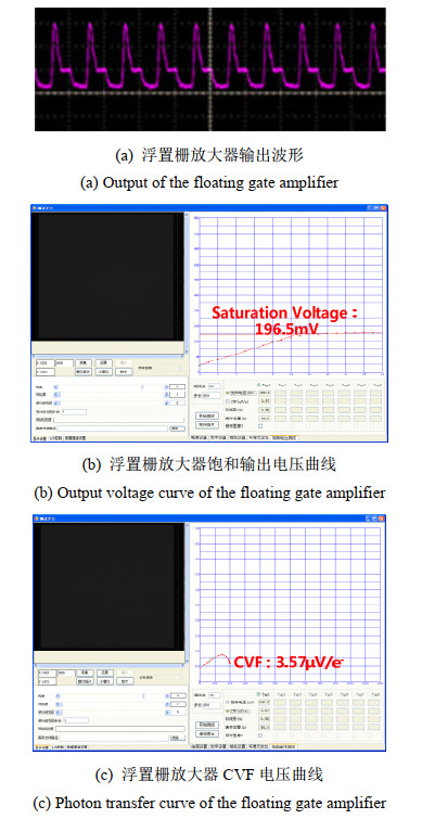
摘要: 本文设计制作了一款阵列规模为1024×1024元、像元尺寸为10 μm×10 μm的昼夜兼容成像EMCCD(electron multiplying charge coupled device),该器件包含国内首次制作的浮置栅放大器,该放大器电荷转换因子(Charge to voltage factor,CVF)为3.57 μV/e-,满阱55 ke-,能够非破坏性判断信号强度。该功能使得场景中微光照区域的像素可以选择性地路由至倍增通道输出,而强光照区域的像素会路由至非倍增通道输出,有了这种场景内可切换增益特性,两种输出的信号重新组合,实现高动态成像。同时为了实现器件在强光应用场合的抗光晕功能,器件像元区域采用了纵向抗晕设计,抗晕倍数为200倍,基于此类器件制作的相机能够恰当地在暗视场中呈现明亮的图像。Abstract: A 1024×1024 EMCCD imaging sensor that captures images from sunlight to starlight was designed and fabricated. The pixel size was 10 μm×10 μm. The device includes nondestructive floating gate output amplifier, its charge-to-voltage conversion factor is 3.57 μV/e-, and its charge handling capacity is 55.04 ke-. The nondestructive floating gate output amplifier can sense the amount of charge present in a charge packet without altering the number of electrons in that charge packet. This enables the camera system to determine whether the pixel charge packet is routed through the normal gain output or the EMCCD output based on a user-selectable threshold. The intra-scene switchable gain feature enables wide-scale dynamic imaging. A vertical overflow drain structure suppressed the image blooming by 200×. This feature enables imaging under extremely low light, even when bright objects are within a dark scene, thus allowing a single camera to capture quality images from sunlight to starlight.
-

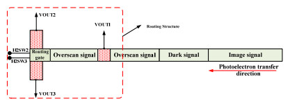
图 2 非倍增/倍增双通道选通结构示意图
Figure 2. Routing process of the non-multiplying and multiplying channels

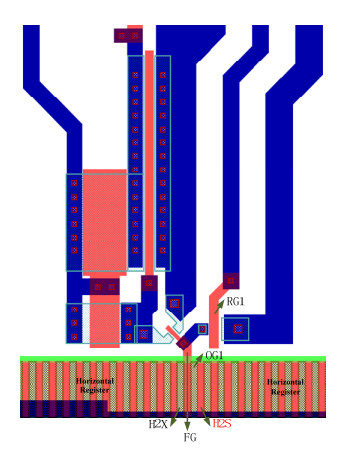
图 4 浮置栅放大器以及浮置扩散放大器结构示意图
Figure 4. Diagram of the floating gate amplifier and floating diffusion amplifier

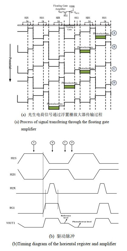
图 6 光生电荷通过非破坏性浮置栅放大器传输
Figure 6. Process and timing diagram of signal transfering through the floating gate amplifier
-
[1] Sudhir K MADAN, Basabi Bhaumik. Experimental Observation of avalanche multiplication in charge-coupled devices[J]. IEEE Trans, Electron Device, 1983, 30(6): 694-699. doi: 10.1109/T-ED.1983.21191 [2] Eric G Stevens, Jeffrey A Clayhold, Hung Doan. Recent enhancements to interline and electron multiplying CCD image sensors[J]. Sensors, 2017, 17: 2841. [3] Parks C, Kosman S, Nelson E. A 30fps 1920×1080 pixel electron multiplying CCD image sensor with per-pixel switchable gain[C]//Proceedings of the 2015 International Image Sensor Workshop (IISW), 2015: 8-11. [4] James R Janesick. Scientific Charge Coupled Devices[M]. USA: SPIE Press, 2001: 585-592. [5] Stevens E G, Burkey B C. A 1-megapixel IL-CCD image sensor with a progressive scan, antiblooming control and lag-free operation[C]//SPIE. Charge-Coupled Device and Solid State Optical Sensors, 1990: 207-216. [6] Eiji Oda, Kenji Nagano, Takanori Tanaka. A 1920(H)×1035(V) pixel high-definition CCD image sensor[J]. Journal of Solid-State Circuits, 1989, 24(3): 711-717. [7] Stephen J Strunk. A progressive scan CCD image sensor for high speed photography[C]//SPIE. Charge-Coupled Device and Solid State Optical Sensors, 1990: 24-35. [8] Oda E, Akiyama I, Kamata T. A 768×490 pixel CCD image sensor[C]// ISSCC Dig. Tech., 1983: 264-265. [9] Albert J P Theuwissen. Solid-State Imaging with CCDs[M]. New York: Kluwer Academic Publishers, 1995. [10] Gareth P Weale, Martin J Kiik, Eric Fox. Anti-Blooming Optimisation using Simulations & Measurements for a VAB Process. IEEE Trans, Electron Device, 2003, 10(3): 186-189. [11] ON semiconductor datasheet. KAE-02150/D 1920(H)×1080(V) Interline CCD Image Sensor[R/OL]. www.onsemi.com , 2015. -

 下载:
下载:


 点击查看大图

图(13)
计量
- 文章访问数: 132
- HTML全文浏览量: 55
- PDF下载量: 33
- 被引次数: 0
