

Infrared Detector Butted Technology for Space
-
摘要: 随着空间遥感相机性能的不断提升,采用更大规模、更多谱段的红外焦平面阵列是未来航天用红外探测器的发展趋势,以满足相机大视场、高分辨率及多光谱探测的能力。目前,单探测器模块的研制受到探测器材料、硅读出电路加工工艺的限制,探测器规模、分辨率、谱段数量等指标无法满足使用要求。因此,通过机械拼接或光学拼接的方式制备大规模、多谱段红外焦平面阵列是必须的工程途经。本文对航天工程用大规模、多谱段红外探测器拼接方式进行了对比分析,给出了各种常见拼接方式的特点,总结了关键技术和核心指标。Abstract: To meet the demand for wide field of view, high-resolution, and multispectral detection in space applications, more large-scale bands and infrared focal plane arrays will be the future trend in space remote sensing. Currently, the scale and band of massive array detectors are limited by the sizes of detector materials and processing technology of silicon; thus, they are unable to meet the space requirements for wide field of view, high-resolution, and multispectral detection. Obtaining large-scale and multiband detectors through butting is a practical solution. In this paper, several butting techniques are discussed, and their properties, key technologies, and capabilities are presented.
-
Key words:
- large-scale infrared detector /
- butted technology /
- multi-spectral /
- ROIC
-

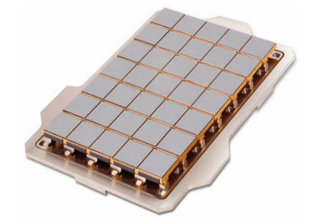
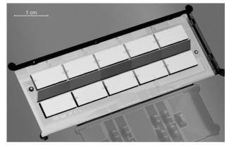
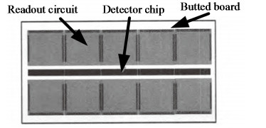
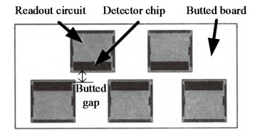
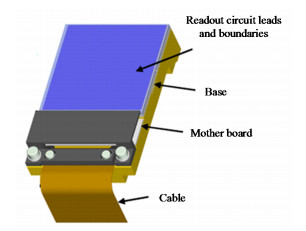
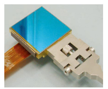
图 1 红外探测器组件机械拼接原理
Figure 1. Mechanical splicing schematic diagram of infrared detector assembly


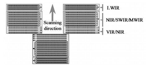
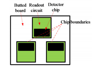
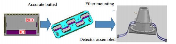
图 20 线列拼接重要边界示意图
Figure 20. Schematic diagram of linear array splicing of important boundaries
表 1 两种拼接特点对比
Table 1. Comparison of two butted technologies
Comparison projects Optical butted Mechanical butted System complexity Complex :
Multiple relay optical systems
Multiple sets of focal plane refrigerator components
Multiple refrigeration controllers and video circuitsSimple :
Relayless optical system
1 set of focal plane refrigerator components
1 set of refrigeration controller and video circuitRequirements for optical system Telecentric image space None Noise equivalent temperature difference High Low Response consistency Low High Focal plane butted accuracy Structure/system assembled required, low accuracy High Focusing structure Several sets 1 set  下载: 导出CSV
-
[1] 刘兆军, 周峰, 李瑜. 航天光学遥感器对红外探测器的需求分析[J]. 红外与激光工程, 2008, 37(1): 25-29. doi: 10.3969/j.issn.1007-2276.2008.01.005LIU Z J, ZHOU F, LI Y. Demands analysis of IR detectors for space remote sensor[J]. Infrared and Laser Engineering, 2008, 37(1): 25-29. doi: 10.3969/j.issn.1007-2276.2008.01.005 [2] 邱民朴, 马文坡. 空间红外推扫成像系统探测器光学拼接方法[J]. 航天返回与遥感, 2019, 40(6): 51-58. doi: 10.3969/j.issn.1009-8518.2019.06.007QIU M P, MA W P. Optical butting of linear infrared detector array for space pushbroom imaging systems[J]. Spacecraft Recovery and Remote Sensing, 2019, 40(6): 51-58. doi: 10.3969/j.issn.1009-8518.2019.06.007 [3] Gert Finger, James W Beletic. Review of the state of infrared detectors for astronomy in retrospect of the June 2002 workshop on scientific detectors for astronomy[C]//Proc. of SPIE, 2003, 4841: 839-852. [4] Philippe Tnbolet, Philippe Chorier. Large infrared focal plane arrays for space applications[J/OL]. [2002-01]. https://www.researchgate.Net/publication/228975841_Large_Infrared_Focal_Plane_Arrays_for_Space_Applications. [5] Peter J Love, Alan W Hoffman, Ken J Ando, et al. 2K×2K HgCdTe detector arrays for VISTA and other applications[C]//Proc. of SPIE, 2004, 5499: 68-77. [6] Reinhold J Dorn, Gert Finger, Gotthard Huster, et al. The CRIRES InSb megapixel focal plane array detector mosaic[C]//Proc of SPIE, 2004, 5499: 510-517. [7] Hall D N B, Luppino G, Hodapp K W, et al. A 4K×4K HgCdTe astronomical camera enabled by the James Webb Space Telescope NIR detector development program[C]//Proc. of SPIE, 2004, 5499: 1-14. [8] Thomas Sprafke, James W Beletic. High-performance infrared focal plane arrays for space applications[J]. Optics and Photonics News, 2008, 19(6): 22-27. doi: 10.1364/OPN.19.6.000022 [9] Thorne P, Gordon J, Hipwood L G, et al. 16 megapixel 12 μm array developments at Selex ES[C]//Proc. of SPIE, 2013, 8704: 87042M-1-87042M-9. [10] Tom Chuh, Markus Loose, David J Gulbransen, et al. Astronomy FPA advancements at Rockwell scientific[C]//Proc. of SPIE, 2006, 6265: 62652K-1-62652K-14. [11] M Zucker, I Pivnik, E Malkinson, et al. Long mid-wave infrared detector with time delayed integration[C]//Proc. of SPIE, 2003, 4820: 580-592. [12] Tribolet P, Chatard J P, Costa P, et al. Progress in HgCdTe homojunction infrared detectors[J]. Journal of Crystal Growth, 1998, 184-185: 1262-1271. doi: 10.1016/S0022-0248(97)00759-8 [13] Robert W Besuner, Christopher J Bebek, Gunther M Haller, et al. A 260 megapixel visible/NIR mixed technology focal plane for space[C]//Proc. of SPIE, 2011, 8155: 81550D-1-81550D-14. [14] Michael Dahlin. Advanced focal plane array systems for next-generation scanning remote sensing instrument[C]// Proc. of SPIE, 2003, 4820: 406-417. [15] 王成刚, 东海杰, 刘泽巍, 等. "高分五号"卫星多谱段集成TDI线列红外探测器[J]. 航天返回与遥感, 2018, 39(3): 80-84. doi: 10.3969/j.issn.1009-8518.2018.03.009WANG C G, DONG H J, LIU Z W, et al. Development of multispectral TDI linear infrared detector for GF-5 satellite[J]. Spacecraft Recovery and Remote Sensing, 2018, 39(3): 80-84. doi: 10.3969/j.issn.1009-8518.2018.03.009 [16] 李言谨, 陈路, 胡晓宁, 等. 长波红外2048元线列碲镉汞焦平面器件[J]. 红外与毫米波学报, 2009, 28(2): 90-92. https://www.cnki.com.cn/Article/CJFDTOTAL-HWYH200902003.htmLI Y J, CHEN L, HU X N, et al. Long-wave infrared 2048-elements linear HgCdTe focal plane array[J]. Journal of Infrared and Millimeter Waves, 2009, 28(2): 90-92. https://www.cnki.com.cn/Article/CJFDTOTAL-HWYH200902003.htm [17] Alan W Hoffman, Elizabeth Corrales, Peter J Love, et al. 2K×2K InSb for astronomy[C]//Proc. of SPIE, 2004, 5499: 59-67. [18] 王成刚, 东海杰. 超长线列碲镉汞红外探测器拼接方式对比分析[J]. 激光与红外, 2013, 43(8): 920-923. doi: 10.3969/j.issn.1001-5078.2013.08.016WANG C G, DONG H J. Butted manner analysis of long linear infrared focal plane detectors of MCT[J]. Laser and Infrared, 2013, 43(8): 920-923. doi: 10.3969/j.issn.1001-5078.2013.08.016 [19] Thorne P, Weller H, Hipwood L G. 12 μm pixel pitch development for 3-side buttable megapixel MW FPAs[C]//Proc. of SPIE, 2012, 8353: 83532J-1-83532J-9. [20] Peter J Love Alan, Hoffman W, David J Gulbransen, et al. Large-format 0.85-2.5 micron HgCdTe detector arrays for low-background applications [C]// Proceeding of SPIE, 2004, 5167: 134-142. [21] 梅强, 曹学强, 张博文, 等. 空间光学相机焦面拼接热变形对图像配准影响[J]. 航天返回与遥感, 2021, 42(5): 31-38. https://www.cnki.com.cn/Article/CJFDTOTAL-HFYG202105005.htmMEI Q, CAO X Q, ZHANG B W, et al. Analysis of the effect of butting assembly thermal deformation on image registration[J]. Spacecraft Recovery and Remote Sensing, 2021, 42(5): 31-38. https://www.cnki.com.cn/Article/CJFDTOTAL-HFYG202105005.htm [22] 郭楠, 于波, 夏晨晖, 等. 空间光学相机焦面拼接基座高温度稳定性控制[J]. 航天返回与遥感, 2020, 41(4): 64-73. https://www.cnki.com.cn/Article/CJFDTOTAL-HFYG202004009.htmGUO N, YU B, XIA C H, et. Temperature control with high stability for the assembly base of space optical cameras[J]. Spacecraft Recovery and Remote Sensing, 2020, 41(4): 64-73. https://www.cnki.com.cn/Article/CJFDTOTAL-HFYG202004009.htm [23] 周峰, 刘冰, 王成刚, 等. 一种红外探测器超大面阵复合拼接方法: CN106813781A[P]. 2017.ZHOU F, LIU B, WANG C G, et. A Composite Splicing Method for Super Large Array of Infrared Detectors: CN106813781A[P]. 2017. [24] Rieke G H. NIRCam Detector Overview[EB/OL]. [2017-07-13]. https://jwst-docs.stsci.edu/jwst-near-infrared-camera/nircam-instrumentation/nir-cam-detector-overview. -


 点击查看大图
图(23) / 表(1)
计量
- 文章访问数: 246
- HTML全文浏览量: 89
- PDF下载量: 134
- 被引次数: 0
