

Research Progress on Materials and Devices of HgCdTe p-on-n Double Layer Heterojunction Grown by VLPE
-
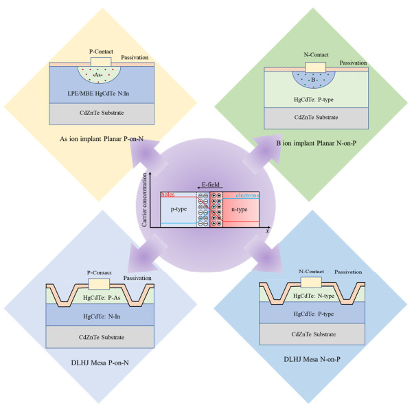
摘要: 本文对比分析了碲镉汞p-on-n器件四种制备方式的优劣,其中,VLPE(Vertical Liquid Phase Epitaxy)技术具有原位As掺杂与高激活率的技术优势,是制备高性能p-on-n双层异质结器件的重要方式。针对该技术,从材料生长、器件工艺和器件性能方面回顾了国内外研究进展,讨论了国内外差距,明确了制约该技术发展的关键问题和技术难点,并提出了解决思路。最后,展望了VLPE技术p-on-n异质结器件的发展趋势。
-
关键词:
- 碲镉汞 /
- p-on-n /
- 台面异质结 /
- 富汞垂直液相外延(VLPE)
Abstract: This paper compares four different fabrication methods for mercury cadmium telluride (HgCdTe) p-on-n devices. Among these methods, vertical liquid-phase epitaxy (VLPE) stands out because of its unique advantages, particularly the high activation rate of in situ arsenic (As) dopants. VLPE is an essential approach for producing high-performance p-on-n double heterojunction devices. This paper reviews the research progress, both domestically and internationally, covering material growth, device processes, and performance. The discrepancies between domestic and foreign research are discussed, and the key challenges and technical bottlenecks hindering VLPE technology development are identified. Several solutions have been proposed to solve this problem. This study provides insights into the future trends of VLPE technology for p-on-n heterojunction devices, which hold significant promise in semiconductor devices.-
Key words:
- HgCdTe /
- p-on-n /
- mesa heterojunction /
- VLPE
-


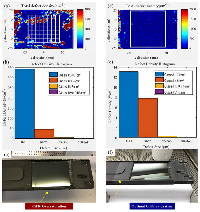
图 4 Cd饱和度对VLPE MCT材料表面缺陷密度的影响:CdTe过饱和时,材料表面缺陷随机分布且缺陷密度较高,石墨舟上附着一层较厚的母液,(a)为CdTe过饱和时表面缺陷分布,(b)为CdTe过饱和时不同大小的表面缺陷的密度统计,(c) CdTe过饱和时石墨舟及碲镉汞薄膜表面形貌;优化CdTe饱和度后,材料表面缺陷密度下降,石墨舟上母液附着层变薄,(d)为CdTe饱和度优化后表面缺陷分布,(e)为CdTe饱和度优化后不同大小的表面缺陷的密度统计,(f) CdTe饱和度优化后石墨舟及碲镉汞薄膜表面形貌[24]
Figure 4. Influence of CdTe saturation on the surface defect density of VLPE MCT materials: When CdTe is oversaturated, surface defects exhibit a random distribution with a relatively high defect density. The graphite boat bears a thick layer of mother liquor. (a) Illustrates the distribution of surface defects during CdTe oversaturation. (b) Provides statistical data on the density of surface defects of varying sizes. (c) Depicts the surface morphology of the graphite boat and the HgCdTe film during CdTe oversaturation. After optimizing CdTe saturation, the material's surface defect density decreases, and the mother liquor layer on the graphite boat. becomes thinner. (d) Shows the surface defect distribution after optimizing CdTe saturation. (e) Presents statistics on the density of surface defects of different sizes.(f) Displays the surface morphology of the graphite boat and the CdTe film after saturation optimization.


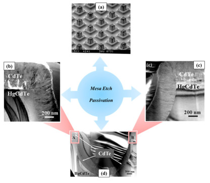
图 7 干法刻蚀与湿法腐蚀结合制备的台面隔离结构:先用低能量、大角度离子刻蚀光刻胶,再用湿化学法腐蚀MCT(a),最后用高能量、小角度离子纵向刻蚀MCT(b),形成高深宽比台面隔离槽(c)[48-49]
Figure 7. Mesa isolation structure prepared by combining dry etching and wet corrosion: first, low-energy, large-angle ion etching is used to remove photoresist, then MCT is corroded by wet chemical method (a), and finally, high-energy, small-angle ion longitudinal etching (b) and high depth-width ratio tabletop isolation trench (c) [48-49]

图 8 p-on-n器件的台面刻蚀与侧壁钝化SEM形貌:台面焦平面阵列[45] (a)以及CdTe钝化层与HgCdTe的界面:(b)台面左侧CdTe/ HgCdTe界面;(c)台面右侧CdTe/ HgCdTe界面;(d)台面底部CdTe/ HgCdT界面[50]
Figure 8. SEM morphology of mesa etching and sidewall passivation of p-on-n devices: Mesa focal plane array (a) and left side interface of CdTe/ HgCdTe (b), right side interface of CdTe/ HgCdTe (c) and bottom side of CdTe/ HgCdTe (d)[50]

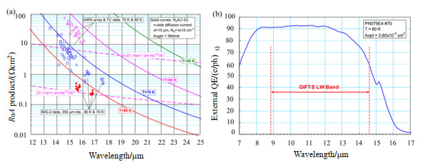
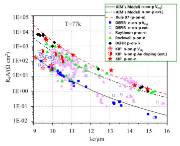
图 9 Raytheon公司基于VLPE技术制备的p-on-n台面结器件在78 K工作温度下R0A与截止波长的关系(a)和量子效率(b)以及应用组件(c)[39-40]
Figure 9. Performance of p-on-n mesa devices based on VLPE technology: (a) relationship between R0A and cut-off wavelength at 78 K operating temperature, (b) quantum efficiency and (c) application components at Raytheon [39-40]


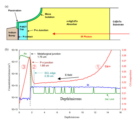
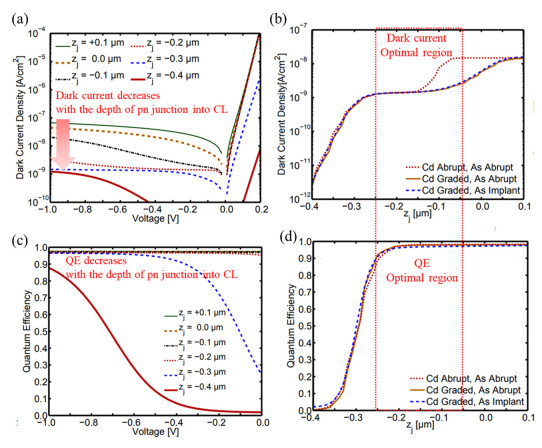
图 12 pn结位置对暗电流和量子效率的影响:(a)为暗电流随pn结进入cap层的深度增加而增大,(b)为暗电流最优区;(c)为量子效率随pn结进入cap层的深度增加而降低,(d)为量子效率最优区[44, 57]
Figure 12. Influence of pn junction position on dark current and quantum efficiency: (a) Shows how dark current increases as the pn junction penetrates the cap layer, (b) represents the optimal region for dark current; (c) quantum efficiency decreases as the pn junction enters the cap layer, (d) depicts the optimal region for quantum efficiency. [44, 57]
-
[1] Lawson W, Nielsen S, Putley E, et al. Preparation and properties of HgTe and mixed crystals of HgTe-CdTe[J]. Journal of Physics and Chemistry of Solids, 1959, 9(3-4): 325-329. doi: 10.1016/0022-3697(59)90110-6 [2] Capper P. Properties of narrow-gap cadmium-based compounds[J]. Optoelectronics IEE Proceedings, 1994, 142(6): 315. [3] LEI W, Antoszewski J, Faraone O. Progress, challenges, and opportunities for HgCdTe infrared materials and detectors[J]. Applied Physics Reviews, 2015, 2(4): 041303. doi: 10.1063/1.4936577 [4] Paul W Kruse, Laurence D McGlauchlin, Richmond B McQuistan. Elements of Infrared Technology[M]. New York: Wiley, 1962. [5] Rogalski A, Martyniuk P, Kopytko M, et al. Trends in performance limits of the hot infrared photodetectors[J]. Applied Sciences-Basel, 2021, 11(2): 501. doi: 10.3390/app11020501 [6] Kinch M A. The future of infrared; Ⅲ–Vs or HgCdTe?[J]. Journal of Electronic Materials, 2015, 44(9): 1-8. [7] 孔金丞, 李艳辉, 杨春章, 等. 昆明物理研究所分子束外延MCT薄膜技术进展[J]. 人工晶体学报, 2020, 49(12): 2221-2229. doi: 10.3969/j.issn.1000-985X.2020.12.002KONG Jincheng, LI Yanhui, YANG Chunzhang, et al. Progress in MBE growth of HgCdTe at kunming institute of physics[J]. Journal of Synthetic Crystals, 2020, 49(12): 2221-2229. doi: 10.3969/j.issn.1000-985X.2020.12.002 [8] 杨建荣. 碲镉汞材料物理与技术[M]. 北京: 国防工业出版社, 2012.YANG Jianrong. Physics and Technology of HgCdTe Materials[M]. Beijing: National Industry Press, 2012. [9] 宋林伟, 孔金丞, 李东升, 等. 金掺杂碲镉汞红外探测材料及器件技术[J]. 红外技术, 2021, 43(2): 97-103. http://hwjs.nvir.cn/article/id/587d68b6-af54-476a-b0b8-5a5e4ef674fdSONG Linwei, KONG Jincheng, LI Dongsheng, et al. Au-doped HgCdTe infrared material and device technology[J]. Infrared Technology, 2021, 43(2): 97-103. http://hwjs.nvir.cn/article/id/587d68b6-af54-476a-b0b8-5a5e4ef674fd [10] Jones C L, Hipwood L G, Shaw C J, et al. High-performance MW and LW IRFPAs made from HgCdTe grown by MOVPE[J]. Proceedings of SPIE. International Society for Optics and Photonics, 2006, 6206: 620610-1-12. [11] Kinch M A. HDVIPTM FPA technology at DRS[C]//Proceedings of SPIE - International Society for Optics and Photonics, 2001, 4369: 566-578. [12] 李立华, 熊伯俊, 杨超伟, 等. p-on-n长波, 甚长波碲镉汞红外焦平面器件技术研究[J]. 红外与毫米波学报, 2022, 41(3): 534-539. https://www.cnki.com.cn/Article/CJFDTOTAL-HWYH202204001.htmLI Lihua, XIONG Bojun, YANG Chaowei, et al. Research on p-on-n LWIR and VLWIR HgCdTe infrared focal plane detectors technology[J]. Journal of Infrared and Millimeter Waves, 2022, 41(3): 534-539. https://www.cnki.com.cn/Article/CJFDTOTAL-HWYH202204001.htm [13] Ashley T, Elliott C T. Non-equilibrium devices for infrared detection[J]. Electronics Letters, 1985, 21(10): 451-452. doi: 10.1049/el:19850321 [14] 俞见云, 孔金丞, 覃钢, 等. 基于非平衡模式的碲镉汞高工作温度探测器[J]. 红外技术, 2023, 45(1): 15-22. http://hwjs.nvir.cn/article/id/f6eb8c94-ee87-4451-babe-88c97d41e4b3YU Jianyun, KONG Jincheng, QIN Gang, et al. High operation temperature non-equilibrium photovoltaic HgCdTe devices[J]. Infrared Technology, 2023, 45(1): 15-22. http://hwjs.nvir.cn/article/id/f6eb8c94-ee87-4451-babe-88c97d41e4b3 [15] Klipstein P. XBn barrier photodetectors for high sensitivity and high operating temperature infrared sensors[C]//Proceedings of SPIE - The International Society for Optical Engineering, 2008, 6940: 69402U. [16] Klipstein P. Depletion-less photodiode with suppressed dark current and method for producing the same[P]. United States Patent 7795640, [2010-09-14]. [17] Gravrand O, Mollard L, Largeron C, et al. Study of LWIR and VLWIR focal plane array developments: comparison between p-on-n and different n-on-p technologies on LPE HgCdTe[J]. Journal of Electronic Materials, 2009, 38(8): 1733-1740. doi: 10.1007/s11664-009-0795-2 [18] Casselman T N. Calculation of the Auger lifetime in degenerate n-type (Hg, Cd)Te[C]//Physics of Narrow Gap Semiconductors, 1982, 152(4): 147-151. [19] Casselman T N. Calculation of the Auger lifetime in p-type Hg1-xCdxTe[J]. Journal of Applied Physics, 1981, 52(2): 848-854. doi: 10.1063/1.328426 [20] Jozwikowski K, Jozwikowska A. The influence of shallow donor and acceptor states on carriers' lifetime in long wavelength HgCdTe infrared detectors[J]. Infrared Physics and Technology, 2021, 117: 103853. doi: 10.1016/j.infrared.2021.103853 [21] Kopytko M, Rogalski A. Figure of merit for infrared detector materials[J]. Infrared Physics and Technology, 2022, 122: 104063. doi: 10.1016/j.infrared.2022.104063 [22] 覃钢, 吉凤强, 夏丽昆, 等. 碲镉汞高工作温度红外探测器[J]. 红外与激光工程, 2021, 50(4): 20200328-1-20200328-11.QIN Gang, JI Fengqiang, XIA Likun, et al. HgCdTe high operation temperature infrared detectors[J]. Infrared and Laser Engineering, 2021, 50(4): 20200328-1-20200328-11. [23] Kopytko M, Rogalski A. New insights into the ultimate performance of HgCdTe photodiodes[J]. Sensors and Actuators A: Physical, 2022, 339: 113511. doi: 10.1016/j.sna.2022.113511 [24] Vilela M F, Hogan J, Fennell B T, et al. Infinite-Melt vertical liquid-Phase epitaxy of HgCdTe from Hg solution: from VLWIR to SWIR[J]. Journal of Electronic Materials, 2022, 51(9): 4731-4741. doi: 10.1007/s11664-022-09810-5 [25] 沈川, 陈路, 卜顺栋, 等. 高温热退火对多层P-on-N结构HgCdTe的界面影响[J]. 红外与毫米波学报, 2021, 40(2): 156-160. https://www.cnki.com.cn/Article/CJFDTOTAL-HWYH202102004.htmSHEN Chuan, CHEN Lu, BU Shundong, et al. Effect of thermal annealing on the interface changes of multi-layer HgCdTe P-on-N materials grown by MBE[J]. J. Infrared Millim. Waves, 2021, 40(2): 156-160. https://www.cnki.com.cn/Article/CJFDTOTAL-HWYH202102004.htm [26] Wenus J, Rutkowski J, Rogalski A. Two-dimensional analysis of double-layer heterojunction HgCdTe photodiodes[J]. IEEE Transactions on Electron Devices, 2001, 48(7): 1326-1332. doi: 10.1109/16.930647 [27] 陈正超, 唐利斌, 郝群, 等. HgCdTe多层异质结红外探测材料与器件研究进展[J]. 红外技术, 2022, 44(9): 889-903. http://hwjs.nvir.cn/article/id/69c43112-b6de-4310-b0fb-9d509cd06375CHEN Zhengchao, TANG Libin, HAO Qun, et al. Research progress on infrared detection materials and devices of HgCdTe multilayer heterojunction[J]. Infrared Technology, 2022, 44(9): 889-903. http://hwjs.nvir.cn/article/id/69c43112-b6de-4310-b0fb-9d509cd06375 [28] Lovecchio P, Wong K, Parodos T, et al. Advances in liquid phase epitaxial growth of Hg1-xCdxTe for SWIR through VLWIR photodiodes[J/OL]. Infrared Detector Materials and Devices, 2004: 65-72. https://www.researchgate.net/publication/253633857_Advances_in_liquid_phase_epitaxial_growth_of_Hg1-xCdxTe_for_SWIR_through_VLW IR_photodiodes .[29] LI X, WANG X, ZHOU S, et al. Comparative study on dark current mechanisms of n-on-p and p-on-n long-wavelength HgCdTe infrared detectors[J]. Infrared Physics & Technology, 2022, 123: 104166. [30] Reibel Y, Rubaldo L, Bonnouvrier G, et al. Latest developments in advanced MCT infrared cooled detectors[C]//Electro-Optical and Infrared Systems: Technology and Applications Ⅷ, 2011: 15-26. [31] Castelein P, Baier N, Gravrand O, et al. Latest developments in the p-on-n HgCdTe architecture at DEFIR[C]//Infrared Technology and Applications XL, 2014: 853-866. [32] Lutz H, Breiter R, Figgemeier H, et al. Improved high operating temperature MCT MWIR modules[C]//Infrared Technology and Applications XL, 2014: 395-406. [33] Tennant W, Lee D, Zandian M, et al. MBE HgCdTe technology: a very general solution to IR detection, described by "Rule 07", a very convenient heuristic[J]. Journal of Electronic Materials, 2008, 37(9): 1406-1410. doi: 10.1007/s11664-008-0426-3 [34] 覃钢, 李东升. 分子束外延碲镉汞薄膜的砷掺杂技术[J]. 红外技术, 2015, 37(10): 858-863. http://hwjs.nvir.cn/article/id/hwjs201510010QIN Gang, LI Dongsheng. The As-doping technique of HgCdTe thin film by MBE[J]. Infrared Technology, 2015, 37(10): 858-863. http://hwjs.nvir.cn/article/id/hwjs201510010 [35] Arias J, Zandian M, Pasko J, et al. Molecular beam epitaxy growth and insitu arsenic doping of p-on-n HgCdTe heterojunctions[J]. Journal of Applied Physics, 1991, 69(4): 2143-2148. doi: 10.1063/1.348741 [36] Capper P, Whiffin P A C, Easton B C, et al. Group Ⅴ acceptor doping of CdxHg1-xTe layers grown by metal-organic vapour phase epitaxy[J]. Materials Letters, 1988, 6: 365-368. doi: 10.1016/0167-577X(88)90125-5 [37] Hipwood L G, Baker I M, Jones C L, et al. LW IRFPAs made from HgCdTe grown by MOVPE for use in multispectral imaging[J]//Infrared Technology and Applications XXXIV, 2008, 6940: 69400G-69400G-8. [38] Bubulac L O. Defect, diffusion and activation in ion implanted HgCdTe[J]. Journal of Crystal Growth, 1988, 86: 723-734. doi: 10.1016/0022-0248(90)90799-Q [39] Gilmore A S, Bangs J, Gerrish A, et al. Advancements in HgCdTe VLWIR materials[C]//Infrared Technology and Applications XXXI, 2005: 5783, DOI: 10.1117/12.607604 .[40] Bratt P, Johnson S, Rhiger D, et al. Historical perspectives on HgCdTe material and device development at raytheon vision systems[C]//Infrared Technology and Applications XXXV, 2009, 7298: 1044-1078. [41] Reine M B. History of HgCdTe infrared detectors at BAE systems[C]//Infrared Technology and Applications XXXV, 2009, 7298: 995-1020. [42] 李向阳, 方家熊. 碲镉汞p-on-n光伏器件优化掺杂的理论计算[J]. 红外与毫米波学报, 2002, 21(1): 71-73. https://www.cnki.com.cn/Article/CJFDTOTAL-HWYH200201016.htmLI Xiangyang, FANG Jiaxiong. Theoretical calculation of doping optimization for p-on-n HgCdTe photodiode[J]. Journal of Infrared and Millimeter Waves, 2002, 21(1): 71-73. https://www.cnki.com.cn/Article/CJFDTOTAL-HWYH200201016.htm [43] Prigozhin I, Zhu M, Bellotti E. Numerical modeling of graded bandgap long wavelength infrared HgCdTe avalanche photodiodes[J]. IEEE Transactions on Electron Devices, 2022, 69(7): 3791-3797. doi: 10.1109/TED.2022.3177701 [44] Schuster J, Dewames R, Wijewarnasuriya P. Dark currents in a fully-depleted LWIR HgCdTe P-on-n heterojunction: analytical and numerical simulations[J]. Journal of Electronic Materials, 2017, 46: 6295-6305. doi: 10.1007/s11664-017-5736-x [45] Reine M B, Tobin S P, Norton P W, et al. Very long wavelength (>15µm) HgCdTe photodiodes by liquid phase epitaxy[J]. Infrared Detector Materials and Devices, 2004, 5564: 54-64. doi: 10.1117/12.557317 [46] Stobie J, Hairston A, Tobin S, et al. VLIWR HgCdTe staring focal plane array development[C]//Proceedings of SPIE - Infrared Systems & Photoelectronic Technology Ⅱ, 2007, 6660: 66600L-1-10. [47] Hutchins M, Smith F, Tobin S, et al. Improved operability in Hg 1-xCdxTe detector arrays[J]. Journal of Electronic Materials, 1999, 28: 624-629. doi: 10.1007/s11664-999-0045-7 [48] Smith E, Venzor G, Newton M, et al. Inductively coupled plasma etching for large format HgCdTe focal plane array fabrication[J]. Journal of Electronic Materials, 2005, 34: 746-753. doi: 10.1007/s11664-005-0014-8 [49] Benson J, Stoltz A, Varesi J, et al. Determination of the ion angular distribution for electron cyclotron resonance plasma-etched HgCdTe trenches[J]. Journal of Electronic Materials, 2004, 33: 543-551. doi: 10.1007/s11664-004-0044-7 [50] ZHAO W, Cook J, Parodos T, et al. Microstructural characterization of CdTe surface passivation layers[J]. Journal of Electronic Materials, 2010, 39: 924-929. doi: 10.1007/s11664-010-1176-6 [51] Reine M, Tobin S, Norton P, et al. Predicted performance of HgCdTe photodiodes for 15-25 µm detection[C]//Infrared Technology and Applications XXXI, 2005, 5783: 211-222. [52] Maschhoff K R. AIRS-Light instrument concept and critical technology development[C]//Infrared Spaceborne Remote Sensing X, 2002: 242-249. [53] Krueger E E, Lee D, Miller C R, et al. HgCdTe photodiodes with cutoff wavelengths of 17 μm at 70 K for use in high-resolution interferometers for remote sensing[C]//Infrared Spaceborne Remote Sensing Ⅴ, 1997: 355-372. [54] 田震, 宋淑芳, 王小菊, 等. 碲镉汞p-on-n长波异质结探测器材料的制备研究[J]. 激光与红外, 2018, 48(6): 730-734. doi: 10.3969/j.issn.1001-5078.2018.06.012TIAN Zhen, SONG Shufang, WANG Xiaoju, et al. Study on fabrication of p-on-n LW HgCdTe heterostructure materials[J]. Laser & Infrared, 2018, 48(6): 730-734 doi: 10.3969/j.issn.1001-5078.2018.06.012 [55] 孔金丞, 宋林伟, 起文斌, 等. 昆明物理研究所大面积水平推舟液相外延碲镉汞薄膜技术进展[J]. 红外技术, 2023, 45(2): 111-122. http://hwjs.nvir.cn/article/id/7df58940-e7fc-43a8-abd4-1d5101fcd692KONG Jincheng, SONG Linwei, QI Wenbin, et al. Progress in LPE growth of HgCdTe at kunming institute of physics[J]. Infrared Technology, 2023, 45(2): 111-122. http://hwjs.nvir.cn/article/id/7df58940-e7fc-43a8-abd4-1d5101fcd692 [56] 宋林伟, 孔金丞, 赵鹏, 等. Au掺杂碲镉汞长波探测器技术研究[J]. 红外与激光工程, 2023, 52(4): 20220655. https://www.cnki.com.cn/Article/CJFDTOTAL-HWYJ202304001.htmSONG Linwei, KONG Jincheng, ZHAO Peng, et al. Research of Au-doped LWIR HgCdTe detector[J]. Infrared and Laser Engineering, 2023, 52(4): 20220655. https://www.cnki.com.cn/Article/CJFDTOTAL-HWYJ202304001.htm [57] Schuster J, Dewames R, Decuir Jr E, et al. Heterojunction depth in P+-on-n eSWIR HgCdTe infrared detectors: generation-recombination suppression[C]//Infrared Sensors, Devices, and Applications Ⅴ, 2015: 7-18. -

 下载:
下载:


 点击查看大图
计量
- 文章访问数: 66
- HTML全文浏览量: 12
- PDF下载量: 46
- 被引次数: 0
