

Characterization and Analysis of Interface Characteristics of InAs/GaSb Type-II Superlattice Materials
-
摘要: 本文系统地介绍了国内外研究机构对超晶格界面进行研究时采用的测试分析手段。其中,通过拉曼光谱、高分辨率透射电子显微镜(HRTEM)、扫描隧道显微镜(STM)、二次离子质谱(SIMS)、X射线光电子能谱(XPS)等测试方法可以对InAs/GaSb II类超晶格材料界面类型、界面粗糙度、陡峭性等特性进行测试分析,从而评估超晶格界面质量。光致发光谱(PL谱)、高分辨率X射线衍射(HRXRD)、霍尔测试、吸收光谱等测试方法则可以研究超晶格界面质量对超晶格材料能带、晶体质量、光学性质的影响。
-
关键词:
- InAs/GaSb II类超晶格 /
- InSb-like界面 /
- GaAs-like界面 /
- 陡峭性
Abstract: This article systematically introduces the testing and analysis methods used by domestic and foreign research institutions to study the superlattice interface. To evaluate the quality of the superlattice interface, the InAs/GaSb type-II superlattice interface type, interface roughness, abruptness, and other characteristics can be tested and analyzed using Raman spectroscopy, high-resolution transmission electron microscopy, a scanning tunneling microscope, secondary ion mass spectroscopy, and X-ray photoelectron spectroscopy. Photoluminescence spectroscopy, high-resolution X-ray diffraction, Hall measurements, and absorption spectroscopy can be used to study the effect of the superlattice interface quality on the energy band, crystal quality, and optical properties of superlattice materials.-
Key words:
- InAs/GaSb type-II superlattice /
- InSb-like interface /
- GaAs-like interface /
- abruptness
-

图 1 在(0 0 1)GaAs上生长的InAs或GaSb缓冲层具有InSb或GaAs IF的InAs/GaSb SL的室温拉曼光谱[16]
Figure 1. Room-temperature Raman spectrum of InAs/GaSb SLs with InSb- or GaAs-like IFs grown on(0 0 1)GaAs using either InAs or GaSb buffer layers

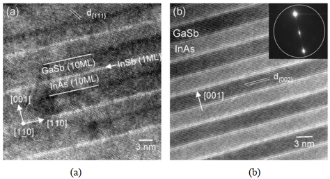
图 2 在GaSb(0 0 1)上生长的InAs/GaSb超晶格的HRTEM图像: (a)沿着[1 1 0]区轴向的InAs/InSb/GaSb SL的横截面HRTEM图像;(b)SL的(0 0 2)晶格条纹图像[17]
Figure 2. HRTEM image of InAs/GaSb superlattice grown on GaSb(0 0 1): (a)Cross-sectional HRTEM images of the InAs/InSb/GaSb SL taken along the [1 1 0] zone axis;(b) Corresponding(0 0 2)lattice fringe image of the SL

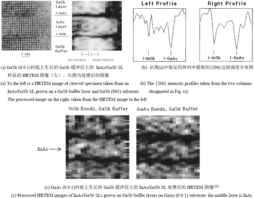
图 3 GaSb(0 0 1)或GaAs(0 0 1)衬底上生长的GaSb缓冲层上的InAs/GaSb SL样品的HRTEM图像
Figure 3. HRTEM images of InAs/GaSb SL samples on GaSb buffer layer grown on GaSb(0 0 1) or GaAs(0 0 1) substrate

图 4 InAs/GaSb超晶格样品的XSTM图像: (a) InAs/GaSb超晶格样品在(110)横截面的InAs-on-GaSb和GaSb-on-InAs界面的阴离子亚晶格的原子分辨率STM图像[19];(b) Pb(As)= 5.3×10⁻⁶ Torr下生长的InAs/GaSb超晶格的XSTM(cross-sectionalscanning tunneling microscopy)图像[20]
Figure 4. XSTM images(anion sublattice) of InAs/GaSb SL samples: (a) STM images(anion sublattice) of InAs/GaSb SL samples in(1 1 0) cross section. As2-soak times are 0 s(bottom), 4 s(middle), and 15 s(top), respectively;(b) XSTM image of a GaSb/ InAs superlattice grown with Pb=5.3×10⁻⁶ Torr revealing the anion sublattice(60 nm×60 nm). Inset: Close-up(7 nm×7 nm) of an InAs/GaSb interface where a segment of GaAs interfacial bonds are observed(dark area indicated by the arrow)

图 5 GaSb层上生长的InAs层的SIMS测试: (a) GaSb层上生长的InAs层的SIMS深度剖面[21];(b) 通过SIMS测量在不同衬底温度下生长的两个InAs on GaSb界面的Sb分布[22]
Figure 5. SIMS of InAs layer growing on GaSb layer: (a) SIMS depth profile of an InAs layer buried in GaSb;(b) Sb profile measured by SIMS for two InAs-grown-on-GaSb interfaces at substrate temperatures of 475℃(dashed line) and 380℃(solid line)

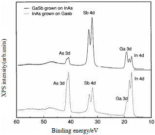
图 6 GaSb/InAs和InAs/GaSb异质结构的代表性的XPS[22]
Figure 6. Representative XPS scans of GaSb/InAs and InAs/ GaSb scans used heterostructures. Measured variation in XPS peak intensity ratios, for both InAs/GaSb and GaSb/InAs growth orders

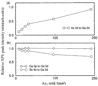
图 7 GaSb表面的As2暴露的XPS峰强度比[22]
Figure 7. XPS peak intensity ratios for As2 exposures of GaSb surfaces

图 8 T=80 K,10MLs-InAs/nInSb ML-InSb/10MLs-GaSb SLs的PL谱[29]
Figure 8. PL spectra of the 10MLs-InAs/nInSb ML-InSb/10MLs GaSb SLs collected at T=80 K. Inset: interface bandege alignment diagram at scale taking into account the inserted InSb layer at the InAs/GaSb heterointerface

图 9 TPL=10 K,在InAs-on-GaSb界面为GaAs-like界面的超晶格材料的PL谱[30]
Figure 9. TPL=10 K PL spectra for SLs structures grown at different As-soak times at InAs-on-GaSb interfaces(GaAs-like interfaces)

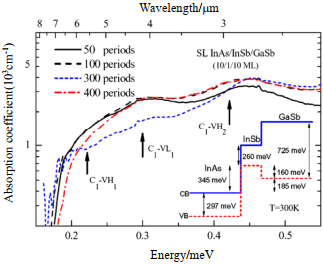
图 10 InAs/InSb/GaSb(10/1/10 MLs)超晶格的RT吸收光谱[17]
Figure 10. RT measured absorption coefficient of strain compensated InAs/InSb/GaSb(10/1/10MLs)SLs
表 1 GaSb/InAs和InAs/GaSb界面的同一侧上的元素之间的XPS峰强度比率[22]
Table 1. XPS peak intensity ratios between elements primarily on the same side of the interface of GaSb/InAs and InAs/GaSb
Structure Measured range of XPS peak area ratios Sb 4d/Ga 3d As 3d/In 4d GaSb/InAs
4g: 7s1.20-1.31 0.63-0.86 InAs/GaSb
12g: 17s0.55-1.24 0.81-1.37 Note: The notation xg: ys specifies x growths and y XPS scans used to obtain a given set of values  下载: 导出CSV
表 2 (InAs + IF)/(GaSb + IF) SLs插入InSb-like或/和GaAs-like界面的数据汇总[34]
Table 2. Data summary of(InAs+IF)/(GaSb+IF) SLs: the InSb-like or/and GaAs-like IFs were inserted between the layers and their values were estimated from shutter time
IF type Period/Å Strain/% Rs/(Ω/sq) ns/(×1011cm−2) μ/(cm2/Vs) 0/0 44.8 −0.13 8563 1.8 4104 InSb/GaAs 45.4 −0.08 3409 2.8 6579 InSb/InSb 45.5 +0.10 7020 2.0 4343 GaAs/GaAs 45.2 −0.30 7675 1.5 5548 GaAs/InSb 45.1 −0.15 45690 52.2 26 Note: The Rs, ns, and μ represent the 10 K resistivity, hole density, and in-plane hole mobility
下载: 导出CSV
-
[1] Chang L L, Saihalasz G A, Esaki L, et al. Spatial separation of carriers in InAs-GaSb superlattices[J]. Journal of Vacuum Science and Technology, 1981, 19(3): 589-591. doi: 10.1116/1.571134 [2] Brum J A, Voisin P, Bastard G, et al. Transient photovoltaic effect in semiconductor superlattices[J]. Physical Review B, 1986, 33(2): 1063-1066. doi: 10.1103/PhysRevB.33.1063 [3] Smith D L, Mailhiot C. Proposal for strained type II superlattice infrared detectors[J]. Journal of Applied Physics, 1987, 62(6): 2545-2548. doi: 10.1063/1.339468 [4] Hood A, Hoffman D, WEI Y, et al. Capacitance-voltage investigation of high-purity InAs/GaSb superlattice photodiodes[J]. Applied Physics Letters, 2006, 88(5): 052112. doi: 10.1063/1.2172399 [5] Hoffman D, Gin A, Wei Y, et al. Negative and positive luminescence in midwavelength infrared InAs-GaSb superlattice photodiodes[J]. IEEE Journal of Quantum Electronics, 2005, 41(12): 1474-1479. doi: 10.1109/JQE.2005.858783 [6] Szmulowicz F, Haugan H J, Brown G J, et al. Interfaces as design tools for short-period InAs/GaSb type-II superlattices for mid-infrared detectors[J]. Opto-electronics Review, 2006, 14(1): 69-75. [7] Christol P, Konczewicz L, Cuminal Y, et al. Electrical properties of short period InAs/GaSb superlattice[J]. Physica Status Solidi(c), 2007, 4(4): 1494-1498. [8] Nesher O, Klipstein P C. High-performance IR detectors at SCD present and future[J]. Opto-electronics Review, 2006, 14(1): 59-68. [9] Szmulowicz F, Haugan H J, Brown G J, et al. Interfaces as design tools for short-period InAs/GaSb type-II superlattices for mid-infrared detectors [J]. Opto-Electronics Review, 2006, 14(1): 69-75. [10] WEI Y J, Razeghi M. Modeling of type-II InAs/GaSb superlattices using an empirical tight-binding method and interface engineering[J]. Physical Review B, 2004, 69(8): 085316. doi: 10.1103/PhysRevB.69.085316 [11] Luna E, Satpati B, Rodriguez J B, et al. Interfacial intermixing in InAs/GaSb short-period-superlattices grown by molecular beam epitaxy[J]. Appl. Phys. Lett., 2010, 96(2): 021904. doi: 10.1063/1.3291666 [12] Sarusi G. QWIP or other alternative for third generation infrared systems[J]. Infrared Physics & Technology, 2003, 44(5): 439-444. [13] Thibado P M, Bennett B R, Twigg M E, et al. Origins of interfacial disorder in GaSb/InAs superlattices[J]. Applied Physics Letters, 1995, 67(24): 3578-3580. doi: 10.1063/1.115323 [14] Tahraoui A, Tomasini P, Lassabatere L, et al. Growth and optimization of InAs/GaSb and GaSb/InAs interfaces[J]. Applied Surface Science, 2000, 162: 425-429. [15] Schmitz J, Wagner J, Fuchs F, et al. Optical and structural investigations of intermixing reactions at the interfaces of InAs/AlSb and InAs/GaSb quantum wells grown by molecularbeam epitaxy[J]. Journal of Crystal Growth, 1995, 150: 858-862. doi: 10.1016/0022-0248(95)80061-G [16] Wagner J, Schmitz J, Herres N, et al. InAs/(GaIn)Sb superlattices for IR optoelectronics: strain optimization by controlled interface formation[J]. Physica E-low-dimensional Systems & Nanostructures, 1998, 2(1): 320-324. [17] Satpati B, Rodriguez J B, Trampert A, et al. Interface analysis of InAs/GaSb superlattice grown by MBE[J]. Journal of Crystal Growth, 2007, 301: 889-892. [18] Twigg M E, Bennett B R. Influence of interface and buffer layer on the structure of InAs/GaSb superlattices[J]. Applied Physics Letters, 1995, 67(11): 1609-1611. doi: 10.1063/1.114955 [19] Kaspi R, Steinshnider J, Weimer M. As-soak control of the InAs -on-GaSb interface[J]. Journal of Crystal Growth, 2001, 225(2/4): 544-549. [20] Jackson E M, Boishin G I, Aifer E H, et al. Arsenic cross-contamination in GaSb/InAs superlattices[J]. Journal of Crystal Growth, 2004, 270(3): 301-308. [21] Zborowski J T, Vigliante A, Moss S C, et al. Interface properties of(In, Ga)Sb/InAs heterostructures[J]. Journal of Applied Physics, 1996, 79(11): 8379-8383. doi: 10.1063/1.362557 [22] WANG M W. Study of interface asymmetry in InAs-GaSb hetero- junctions[J]. Journal of Vacuum Science & Technology B, 1995, 13(4): 1689-1693. [23] Booker G R, Klipstein P C, Lakrimi M, et al. Growth of InAs/GaSb strained layer superlattices II[J]. Journal of Crystal Growth, 1995, 146(1-4): 495-502. doi: 10.1016/0022-0248(94)00536-2 [24] Daly M S, Symons D M, Lakrimi M, et al. Interface composition dependence of the band offset in InAs/GaSb[J]. Semiconductor Science and Technology, 1996, 11(5): L823. doi: 10.1088/0268-1242/11/5/001 [25] Young M H, Chow D H, Hunter A T, et al. Recent advances in Ga1−xInxSb/InAs superlattice IR detector materials[J]. Applied Surface Science, 1998, 123-124: 395-399. doi: 10.1016/S0169-4332(97)00490-X [26] Bennett B R, Shanabrook B V, Wagner R J, et al. Interface composition control in InAs/GaSb superlattices[J]. Solid-state Electronics, 1994, 37(4-6): 733-737. doi: 10.1016/0038-1101(94)90288-7 [27] Chow D H, Miles R H, Hunter A T, et al. Effects of interface stoichiometry on the structural and electronic properties of Ga1−x InxSb/InAs superlattices[J]. Journal of Vacuum Science & Technology B, 1992, 10(2): 888-891. [28] 邱永鑫. InAs/GaSb超晶格界面微观结构研究[D]. 哈尔滨: 哈尔滨工业大学, 2008.QIU Yongxin. Study on Interface Microstructure of InAs/GaSb Super- lattice[D]. Harbin: Harbin Institute of Technology, 2008. [29] Rodriguez J B, Christol P, Cerutti L, et al. MBE growth and characterization of type-II InAs/GaSb superlattices for mid-infrared detection[J]. Journal of Crystal Growth, 2005, 274(1): 6-13. [30] Jasik A, Sankowska I, Pierścinska D, et al. Blueshift of bandgap energy and reduction of non-radiative defect density due to precise control of InAs-on-GaSb interface in type-II InAs/GaSb superlattice[J]. Journal of Applied Physics, 2011, 110(12): 123103. doi: 10.1063/1.3671024 [31] Omaggio J P, Meyer J R, Wagner R J, et al. Determination of band gap and effective masses in InAs/Ga1−xInxSb superlattices[J]. Applied Physics Letters, 1992, 61(2): 207-209. doi: 10.1063/1.108219 [32] WANG M W, Collins D A, Mcgill T C, et al. Effect of interface composition and growth order on the mixed anion InAs/GaSb valence band offset[J]. Applied Physics Letters, 1995, 66(22): 2981-2983. doi: 10.1063/1.114250 [33] Haugan H J, Brown G J, Grazulis L, et al. Optimization of InAs/GaSb type-II superlattices for high performance of photodetectors[J]. Physica E: Low-dimensional Systems and Nanostructures, 2004, 20(3-4): 527-530. doi: 10.1016/j.physe.2003.09.003 [34] Haugan H J, Elhamri S, Brown G J, et al. Growth optimization for low residual carriers in undoped midinfrared InAs/GaSb superlattices[J]. Journal of Applied Physics, 2008, 104(7): 240. [35] Szmulowicz F, Haugan H J, Brown G J, et al. Effect of interfaces and the spin-orbit band on the band gaps of InAs/GaSb superlattices beyond the standard envelope-function approximation[J]. Physical Review B, 2004, 69(15): 155321. doi: 10.1103/PhysRevB.69.155321 -


 点击查看大图

计量
- 文章访问数: 149
- HTML全文浏览量: 49
- PDF下载量: 61
- 被引次数: 0
