

As Ion Implantation Technology for LWIR HgCdTe Infrared Detector
-
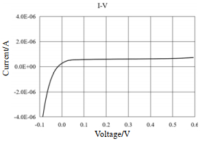
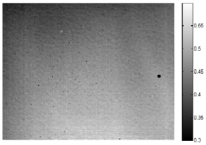
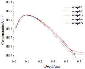
摘要: p-on-n结构的碲镉汞红外探测器具有长的少子寿命、低暗电流、高R0A值等优点,是高温器件、长波甚长波器件发展的重要器件结构。而国内还鲜有砷注入掺杂p-on-n长波HgCdTe探测器的相关报道,为了满足军事、航天等领域对高性能长波探测器迫切的应用需求,针对As离子注入的长波p-on-n碲镉汞红外探测器退火工艺技术进行研究。采用二次离子质谱(SIMS)仪分析注入及退火后As离子浓度分布情况,使用半导体参数测试仪表征pn结的I-V特性。研究结果表明,在富汞0.5 h 430℃+20 h 240℃条件下,实现As激活,成功制备As注入长波15 μm 640×512的p-on-n碲镉汞红外焦平面器件,器件有效像元率大于99.7%。该研究对长波甚长波碲镉汞p-on-n焦平面器件的制备具有重要意义。Abstract: The p-on-n HgCdTe infrared detector has advantages of long minority carrier life, low dark current, high R0A product, and is an important device structure in the development of high-temperature detectors along with long wavelength infrared (LWIR) and very LWIR(VLWIR) detectors. However, there are few local reports on arsenic-implanted doped p-on-n long-wave HgCdTe detectors. To meet the urgent application requirements of high-performance long-wave detectors in the military and aerospace fields, studies have focused on long-wavelength p-on-n HgCdTe infrared detector annealing technology for As ion implantation. Secondary ion mass spectrometry(SIMS) was used to analyze the distribution of As ion concentration after implantation and annealing, and a semiconductor parameter tester was used to characterize the I-V characteristics of the pn junction. The results show that under mercury-rich conditions at 430℃ for 0.5 h and at 240℃ for 20 h, the As was activated. Further, the As implanted long-wavelength 15-μm 640×512 p-on-n HgCdTe infrared focal plane detector was successfully fabricated, and the operable pixel factor of the detector was greater than 99.7%. This research is of great significance for the fabrication of LWIR and VLWIR mercury cadmium telluride p-on-n focal plane detectors.
-
Key words:
- As implantation and doping /
- p-on-n /
- annealing activation /
- MCT(Mercury Cadmium Telluride) /
- SIMS
-
表 1 退火条件
Table 1. Annealing conditions
Sample Energy/keV Dose/
cm-2Annealing conditions Time/h Temperature/℃ 1 300 5E+14 0 0 2 300 5E+14 0.5 360 3 300 5E+14 1 360 4 300 5E+14 2 360 5 300 5E+14 5 360 6 300 5E+14 1 380 7 300 5E+14 0.5 400 8 300 5E+14 1 400 9 300 5E+14 4 400 10 300 5E+14 0.5 430  下载: 导出CSV
表 2 样品1~10的测试数据
Table 2. Test data for samples 1-10
Sample EOR/μm Peak depth/μm Peak concentration/cm-3 1 0.4171 0.0962 3.71E+19 2 0.4182 0.1011 3.6E+19 3 0.4263 0.1050 3.39E+19 4 0.4755 0.1059 3.34E+19 5 0.4812 0.1095 3.27E+19 6 0.4954 0.1134 2.73E+19 7 0.5075 0.1074 3.77E+19 8 0.5263 0.1249 3.02E+19 9 0.5577 0.1280 1.87E+19 10 0.8557 0.1314 8.64E+18
下载: 导出CSV
-
[1] LEI W, Antoszewski J, Faraone L. Progress, challenges, and opportunities for HgCdTe infrared materials and detectors[J]. Applied Physics Reviews, 2015, 2(4): 041303. doi: 10.1063/1.4936577 [2] Rogalski A, Martyniuk P, Kopytko M. Challenges of small-pixel infrared detectors: a review[J]. Reports on Progress in Physics, 2016, 79(4): 046501. doi: 10.1088/0034-4885/79/4/046501 [3] Korotaev A G, Izhnin I I, Mynbaev K D, et al. Hall-effect studies of modificationof HgCdTe surface properties with ion implantation and thermal annealing[J]. Surface & Coatings Technology, 2020, 393: 125721. [4] Bubulac L O, Lo D S, Tennant W E, et al. p on n ion implanted junctions in liquid phase epitaxy HgCdTe layers on CdTe substrates[J]. Applied Physics Letters, 1987, 50(22): 1586-1588. doi: 10.1063/1.97788 [5] Baier N, Cervera C, Gravrand O, et al. Latest developments in long-wavelength and very-long-wavelength infrared detection with p-on-n HgCdTe[J]. Journal of Electronic Materials, 2015, 44(9): 3144-3150. doi: 10.1007/s11664-015-3851-0 [6] Izhnin I I, Fitsych O I, Świątek Z, et al. Effect of annealing on the structural properties of arsenic-implanted mercury cadmium telluride[J]. Opto-Electron Review, 2019, 27(1): 14-17. doi: 10.1016/j.opelre.2019.01.002 [7] Robinson H G, Berding M A, Hamilton W J. Enhanced diffusion and interdiffusion in HgCdTe from Fermi-level effects[J]. Journal of Electronic Materials, 2000, 29(6): 657-663. doi: 10.1007/s11664-000-0201-6 [8] 陈慧卿, 史春伟, 胡尚正, 等. 中波镉汞p-on-n高温工作技术研究[J]. 激光与红外, 2020, 50(4): 435-438. doi: 10.3969/j.issn.1001-5078.2020.04.009CHEN H Q, SHI C W, HU S Z, et al. Study on p-on-n technology of the MWIR HgCdTe for hot work[J]. Laser and Infrared, 2020, 50(4): 435-438. doi: 10.3969/j.issn.1001-5078.2020.04.009 [9] Arias J M, Pasko J G, Zandian M, et al. MBE HgCdTe heterostructure p-on-n planar infrared photodiodes[J]. Journal of Electronic Materials, 1993, 22(8): 1049-1053. doi: 10.1007/BF02817523 [10] Mollard L, Destefanis G, Baier N, et al. Planar p-on-n HgCdTe FPAs by arsenic ion implantation[J]. Journal of Electronic Materials, 2009, 38(8): 1805-1813. doi: 10.1007/s11664-009-0829-9 [11] Schaake H F. Kinetics of activation of group V impurities in Hg1−xCdxTe alloys[J]. Journal of Applied Physics, 2000, 88(4): 1765-1770. doi: 10.1063/1.1302738 [12] Berding M A, Sher A, van Schilfgaarde M, et al. Modeling of arsenic activation in HgCdTe[J]. Journal of Electronic Materials, 1998, 27(6): 605-609. doi: 10.1007/s11664-998-0023-5 [13] Shaw D. An activation model for the As acceptor in HgCdTe[J]. Semiconductor Science Technology, 2008, 23(78): 085014. [14] Baier N, Mollard L, Rothman J, et al. Status of p-on-n HgCdTe technologies at DEFIR[C]//Proceedings of SPIE, The International Society for Optical Engineering, Infrared Technology and Applications XXXV, 2009, 7298: 729823. [15] Bubulac L O. Diffusion and activation of p-type species for p-on-n junction formation and novel characterization techniques for mercury cadmium telluride epilayers[D]. Los Angeles: University of California, 1991. [16] Ryssel H, Lang G, Biersack J P, et al. Ion implantation doping of Cd0.2Hg0.8Te for infrared detectors[J]. IEEE Transactions on Electron Devices, 1980, 27(1): 58-62. doi: 10.1109/T-ED.1980.19819 -


 点击查看大图
图(4) / 表(2)
计量
- 文章访问数: 206
- HTML全文浏览量: 49
- PDF下载量: 89
- 被引次数: 0
