

Investigation of Energy Band Structures of InAs/GaSb and M Structure Superlattices
-
摘要: 本文通过k·p方法研究了传统InAs/GaSb超晶格和M结构超晶格的能带结构。首先,计算了不同周期厚度的InAs/GaSb超晶格的能带结构,得到用于长波超晶格探测器吸收层的周期结构。然后,计算了用于超晶格长波探测器结构的M结构超晶格的能带结构,并给出长波InAs/GaSb超晶格与M结构超晶格之间的带阶。最后,基于能带结构,计算出长波超晶格与M结构超晶格的态密度,进而得出的载流子浓度(掺杂浓度)与费米能级的关系。这些材料参数可以为超晶格探测器结构设计提供基础。
-
关键词:
- k·p方法 /
- InAs/GaSb超晶格 /
- M结构超晶格 /
- 能带结构 /
- 掺杂浓度
Abstract: In this study, the band structures of conventional InAs/GaSb and M structure super lattices are investigated using the k·p method. First, the band structures of InAs/GaSb super lattices with various period thickness are calculated, and the period structure used for a longwave super lattice detector is obtained. Subsequently, the band structure of the M structure super lattice, which is prevalently employed in longwave super lattice infrared detectors, is also calculated. The band offset between a longwave InAs/GaSb super lattice and M structure super lattice is provided. Furthermore, based on the band structures, the relationship between the carrier density (doping density) and the position of the Fermi level for longwave InAs/GaSb and M structure super lattices is obtained. This was followed by a density of states (DOS) calculation. These calculated material parameters can provide the foundation for designing super lattice infrared detectors.-
Key words:
- k·p method /
- InAs/GaSb superlattice /
- M structure super lattice /
- energy band structure /
- doping density
-

图 1 InAs/GaSb超晶格带隙随InAs层厚度的关系
Figure 1. Variation of band gap of InAs/GaSb superlattice with respect to InAs layer thickness.

图 2 7 MLs GaSb/ 1 ML InSb/ 14 MLs InAs/ 1 ML InSb能带带阶排列
Figure 2. Band edge alignment of 7 MLs GaSb/ 1 ML InSb/ 14 MLs InAs/ 1 ML InSb

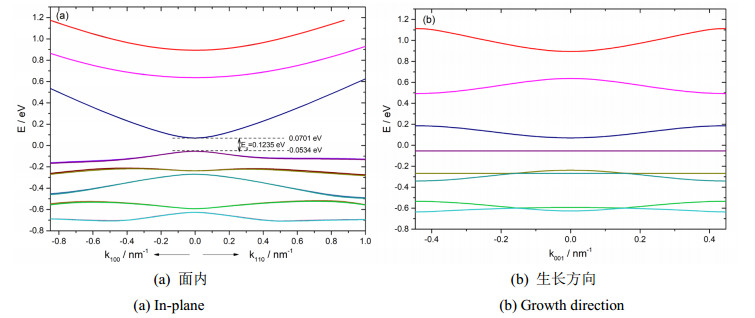
图 3 14 MLs InAs/ 7 MLs GaSb超晶格的能带色散关系,能量原点为GaSb体材料的价带顶
Figure 3. Energy band dispersion of 14 MLsInAs/ 7 MLs GaSb superlattice, the energy origin is set as the top of GaSb valence band

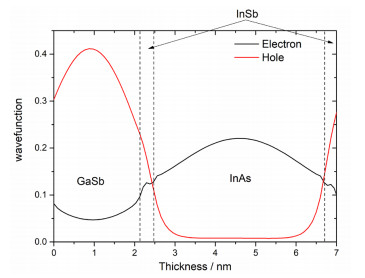
图 4 14 MLs InAs/ 7 MLs GaSb超晶格在单周期内的波函数
Figure 4. Wave function of 14 MLs InAs/ 7 MLs GaSb superlattice in unit cell

图 5 18 MLs InAs / 1 ML InSb/ 3 MLs GaSb / 5 MLs AlSb /3 MLs GaSb/ 1 ML InSb能带带阶排列
Figure 5. Band edge alignment of 18 MLs InAs / 1 ML InSb/ 3 MLs GaSb / 5 MLs AlSb / 3 MLs GaSb/ 1 ML InSb

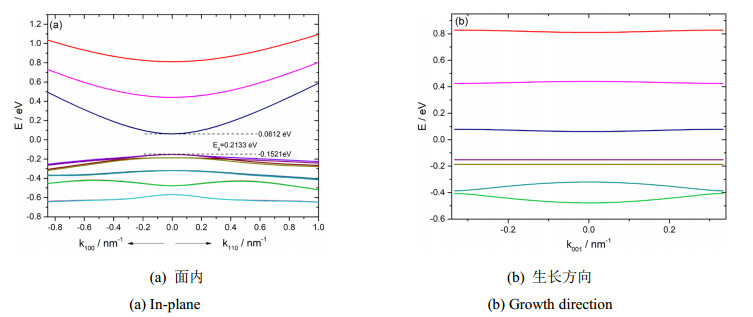
图 6 18 MLs InAs / 3 MLs GaSb / 5 MLs AlSb / 3 MLs GaSb M结构超晶格的能带色散关系,能量原点为GaSb体材料的价带顶
Figure 6. Energy band dispersion of 18 MLs InAs / 3 MLs GaSb / 5 MLs AlSb / 3 MLs GaSb M structure superlattice, the energy origin is set as the top of GaSb valence band

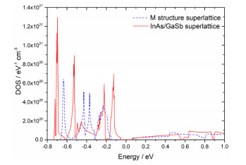
图 7 14 MLs InAs / 7 MLs GaSb超晶格和18 MLs InAs / 3 MLs GaSb / 5 MLs AlSb / 3 MLs GaSbM结构超晶格的态密度
Figure 7. The density of states for 14 MLs InAs / 7 MLs GaSb superlattice and 18 MLs InAs / 3 MLs GaSb / 5 MLs AlSb / 3 MLs GaSb M structure superlattice

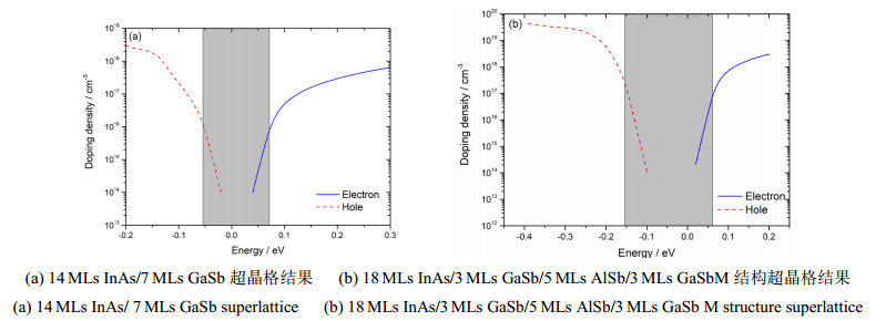
图 8 掺杂浓度与费米能级位置之间的关系
Figure 8. The relationship between doping density and Fermi energy level
表 1 14 MLs InAs/ 7 MLs GaSb超晶格和18 MLs InAs/ 3 MLs GaSb/ 5 MLs AlSb/ 3 MLs M结构超晶格的关键能带参数
Table 1. Critical energy band parameter of 14 MLs InAs/ 7 MLs GaSb superlattice and 18 MLs InAs/ 3 MLs GaSb/ 5 MLs AlSb/ 3 MLs M structure superlattice
Structure Effective energy
gap (Eg)/eVBottom of conduction
band (Ec)/eVTop of valence
band (Ev)/eVΔEc/meV ΔEv/meV 14 MLs InAs/ 7 MLs GaSb superlattice 0.1235 0.0701 -0.0534 -- -- 18 MLs InAs/ 3 MLs GaSb/ 5 MLs AlSb/ 3 MLs M structure superlattice 0.2133 0.0612 -0.1521 -8.9 -98.7  下载: 导出CSV
-
[1] Rhiger D R. Performance Comparison of Long-Wavelength InfraredType Ⅱ Superlattice Devices with HgCdTe[J]. J. Electron Mater. , 2011, 40: 1815. doi: 10.1007/s11664-011-1653-6 [2] Sai Halasz G A, Tsu R, Esaki L. A new semiconductor superlattice[J]. Appl. Phys. Lett. , 1977, 30: 651. doi: 10.1063/1.89273 [3] Smith D L, Mailhiot C. Proposal for strained type Ⅱ superlattice infrared detectors[J]. J. Appl. Phys. , 1987, 62: 2545. doi: 10.1063/1.339468 [4] Youngsdale E R, Meyer J R, Hoffman C A, et al. Auger lifetime enhancement in InAs-Ga1-xInxSb superlattices[J]. Appl. Phys. Lett. , 1994, 64: 3162. doi: 10.1063/1.111325 [5] Rogalski A, Martyniuk P, Kopytko M. InAs/GaSb type-Ⅱ superlattice infrared detectors: Future prospect[J]. Appl. Phys. Rev. , 2017(4): 031304. http://adsabs.harvard.edu/abs/2017ApPRv...4c1304R [6] Nguyen B M, Hoffman D, Delaunay PY, et al. Dark current suppression in type Ⅱ InAs/GaSb superlattice long wavelength infrared photodiodes with M-structure barrier[J]. Appl. Phys. Lett. , 2007, 91: 163511. doi: 10.1063/1.2800808 [7] Gunapala S D, Ting D Z, Hill C J, et al. Demonstration of a 1024×1024 Pixel InAs-GaSb Superlattice Focal Plane Array[J]. IEEE Photon. Technol. Lett. , 2010, 22: 1856. doi: 10.1109/LPT.2010.2089677 [8] Klipstein P C, Avnon E, Benny Y, et al. InAs/GaSb Type Ⅱ superlattice barrier devices with a low dark current and a high quantum efficiency[C]//Proc. of SPIE, 2014, 9070: 90700U. [9] Vurgaftman I, Aifer E H, Canedy C L, et al. Graded band gap for dark-current suppression in long-wave infrared W-structured type-Ⅱ superlattice photodiodes[J]. Appl. Phys. Lett. , 2006, 89: 121114. doi: 10.1063/1.2356697 [10] XU W, LI L L, DONG H M, et al. Band hybridization and spin-splitting in InAs/AlSb/GaSb type Ⅱ and broken-gap quantum wells[J]. J. Appl. Phys. , 2010, 108: 053709. doi: 10.1063/1.3476059 [11] CHUANGS L. Physics of Photonic Devices[M]. New York: Wiley, 2nd ed. 2009. [12] Vurgaftman I, Meyer J R, Ram-Mohan L R. Band parameters for Ⅲ–V compound semiconductors and their alloys[J]. J. Appl. Phys., 2001, 89: 5815. doi: 10.1063/1.1368156 [13] Shun Lien Chuang. Efficient band-structure calculations of strained quantum wells[J]. Phys. Rev. B, 1991, 43: 9649. doi: 10.1103/PhysRevB.43.9649 [14] Nakamura K, Shimizu A, Koshiba M, et al. Finite-element analysis of the miniband structures of semiconductor superlattices with arbitrary periodic potential profiles[J]. IEEE J. Quantum Electron., 1991, 27: 2053. http://ieeexplore.ieee.org/document/83413 [15] Chuang S L, Chang C S. A band-structure model of strained quantum-well wurtzite semiconductors[J]. Semicond. Sci. Technol. , 1997, 12: 252. doi: 10.1088/0268-1242/12/3/004 [16] Davies J H. The Physics of Low-Dimensional Semiconductors: An Introduction[M]. Cambridge: Cambridge University Press, 2005. [17] Frank Fuchs, N Herres, J Schmitz, et al. InAs/GaSb superlattices characterized by high-resolution x-ray diffraction and infrared optical spectroscopy[C]//Proc. of SPIE, 1996, 70: 2554. -


 点击查看大图

计量
- 文章访问数: 407
- HTML全文浏览量: 215
- PDF下载量: 117
- 被引次数: 0
