

The Research Progress in Type Ⅱ Superlattices Infrared Focal Plane Array Detectors
-
摘要: 近几年,二类超晶格红外探测器在材料生长、器件结构设计、器件制备上经历了快速的发展,使得二类超晶格成为除碲镉汞外最受关注的红外探测器材料。本文简要介绍了二类超晶格的优势,总结了国际上二类超晶格红外探测器研究进展,回顾了二类超晶格红外探测器的技术发展历程,并分析了国内二类超晶格材料与器件中存在的技术问题。Abstract: In recent years, the type Ⅱ superlattices (T2SL) infrared detector has experienced incredible improvements in material growth, device structure design, device fabrication techniques, which make the T2SL become the most popular infrared detector material, besides HgCdTe. This article briefly introduces the advantage of the T2SL material, summarizes the international research status in T2SL-based photodetectors, reviews the history of technology development of T2SL-based photodetectors and analyzes the drawback of the research of T2SL material and device technology in China.
-
Key words:
- type Ⅱ superlattices /
- infrared detector /
- focal-plane arrays (FPAs)
-

图 2 AIM InAs/GaSb超晶格中波二极管截面示意图
Figure 2. Schematic cross section of an InAs/GaSb SL MWIR diode of AIM

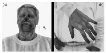
图 3 AIM InAs/GaSb超晶格256×256中波焦平面成像系统拍摄的照片
Figure 3. Thermal images taken with the InAs/GaSb superlattice 256×256 MWIR FPA camera system of AIM

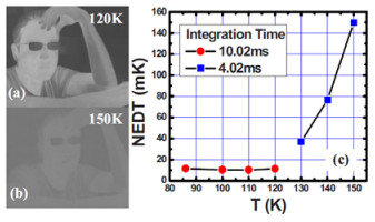
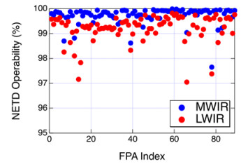
图 4 美国西北大学中波焦平面探测器在120 K(a)和150 K(b)下的成像照片,(c) 86-150 K下焦平面的NTED
Figure 4. Images taken with a MWIR FPA detector of Northwestern University operating at (a) 120 K and (b) 150 K (c) NEDT measured from 86 to150 K

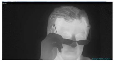
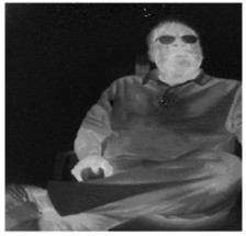
图 5 休斯实验室1 k×2 k/5 μm焦平面在150 K下拍摄的照片
Figure 5. Image captured by a 1 k×2 k/5 μm MWIR FPA of HRL operated at 150 K

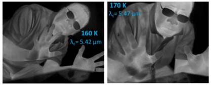
图 6 JPL 640×512规格InAs/InAsSb超晶格中波红外焦平面拍摄的照片
Figure 6. Images taken at 160 K and 170 K using a 640×512 format InAs/InAsSb superlattice MWIR focal plane array of JPL

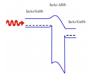
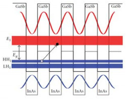
图 7 p-π-M-N超晶格二极管的器件结构与能带图
Figure 7. Device structure and band diagram of a p-π-M-N superlattice photodiode

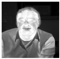
图 8 美国西北大学1 k×1 k长波焦平面在81 K和68 K拍摄的照片
Figure 8. Image taken with the 1 k×1 k LWIR FPA of Northwestern University at 81 K and 68 K

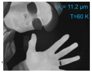
图 10 JPL InAs/GaSb超晶格长波红外焦平面拍摄的照片
Figure 10. Image taken with the InAs/GaSb LWIR superlattice infrared FPA of JPL

图 11 JPL InAs/InAsSb超晶格长波红外焦平面探测器拍摄的照片
Figure 11. Image taken with the InAs/InAsSb LWIR superlattice infrared FPA detector of JPL

图 14 AIM 384×288中波双色二类超晶格焦平面成像效果
Figure 14. Bispectral infrared image taken with 384×288 MWIR dual-band T2SL FPA of AIM

图 15 美国西北大学320×256超晶格中长波双色焦平面拍摄的照片
Figure 15. Imaging taken with 320×256 MWIR-LWIR dual-color T2SL FPA of Northwestern University
(a) MWIR (b) LWIR 
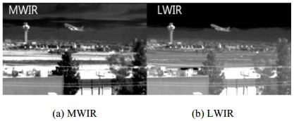
图 16 休斯实验室中长双色焦平面探测器在80 K温度和f/4条件下拍摄的照片
Figure 16. Pictures acquired with a MW/LW FPA of HRL at 80 K and f/4
(a) MWIR (b) LWIR 
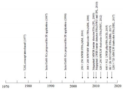
图 18 二类超晶格红外探测器发展历程
Figure 18. Roadmap of type-Ⅱ superlattice infrared photodetectors development
表 1 不同探测波段探测器及焦平面性能参数
Table 1. Performance parameter of detector and FPA under different detection regime
Research Institute Device structure Operation temperature/K Cut-off wavelength/μm Quantum efficiency/% Dark current/A/cm-2 Detectivity/Jones FPA format/pitch NETD/mK Operability/% Publish year MWIR AIM n-i-p 77 5.4
(5% cutoff)30 256×256/40 μm 11.1 99.42 2005 Northwestern University p-π-M-N 150 4.2 1.05×10¹² 320×256 11.0@120 K 2011 HRL 150 5.0 50 without AR coating 6.3×10⁻⁶ 2 k×1 k/5 μm < 20@150 K, f/2.3, with subframe
averaging99.9 2017 JPL nBn 150 5.4 52 4.5×10⁻⁵ 640×512/24 μm 18.7 99.7 2018 LWIR Northwestern University p-π-M-N 77 11.0 >50 5.5×10⁻⁵ 1 k×1 k/18 μm 27 @81 K
19@68 K2010 JPL CBIRD 80 11.5 21 1 k×1 k/17.5 μm 53 2010 JPL nBn 60 11.2 37 1×10⁻⁵ 640×512 21 99.7% 2018 SCD pBp 77 9.5 ~50 4.4×10⁻⁵ 640×512/18 μm 15 (with 8 frame average) >99% 2016 Dual color IR AIM 77 4 (Blue)
5 (Red)2.2×10⁻⁷
1.9×10-7384×288/40 μm 29.5(Blue)
16.5 (Red)2006 Northwestern University 5.2 @160 K for MW
11.2
@77K for LW40-50@160K for MW
> 30
@77K for LW7.0×1012@160K for MW
2.0×10¹¹
@77K for LW320×256 10 (MW)
30 (LW)2012 HRL 80 1280×720/
12μm27.44 (MW)
27.62(LW)99.4(MW)
99.09(LW)2017 Note:Unless otherwise indicated, the cut-off wavelength refers to 50% cut-off wavelength  下载: 导出CSV
-
[1] Sai-halasz G A, Tsu R, Esaki L. A new semiconductor superlattice[J]. Appl. Phys. Lett., 1977, 30: 651. doi: 10.1063/1.89273 [2] Sai-halasz G A, Esaki L, Harrison W A. InAs/GaSb superlattice energy structure and its semiconductor-semimetal transition[J]. Phys. Rev. B, 1978, 18: 2812. doi: 10.1103/PhysRevB.18.2812 [3] Smith D L, Mailhiot C. Proposal for strained type Ⅱ superlattice infrared detectors[J]. J. Appl. Phys., 1987, 62: 2545. doi: 10.1063/1.339468 [4] Johnson J L, Samoska L A, Gossard A C, et al. Electrical and optical properties of infrared photodiodes using the InAs/Ga1−xInxSb superlattice in heterojunctions with GaSb[J]. J. Appl. Phys., 1996, 80: 1116. doi: 10.1063/1.362849 [5] Rogalski A, Kopytko M, Martyniuk P. InAs/GaSb type-Ⅱ superlattice infrared detectors: three decades of development[C]//Proc. of SPIE, 2017, 10117: 1017715. [6] Plis E A, InAs/GaSb type-Ⅱ superlattice detectors[J]. Adv. Electron., 2014, 2014: 246769 [7] 尚林涛, 王静, 邢伟荣, 等. 红外探测Ⅱ类超晶格技术概述(一)[J]. 激光与红外, 2021, 51(4): 404. doi: 10.3969/j.issn.1001-5078.2021.04.002 [8] 尚林涛, 王静, 邢伟荣, 等. 红外探测Ⅱ类超晶格技术概述(二)[J]. 激光与红外, 2021, 51(5): 548. doi: 10.3969/j.issn.1001-5078.2021.05.002 [9] Walther M, Rehm R, Fuchs F, et al, 256×256 Focal Plane Array Midwavelength Infrared Camera Based on InAs/GaSb Short-Period Superlattices[J]. J. Electron. Mater., 2005, 34: 722. doi: 10.1007/s11664-005-0010-z [10] Rehm R, Walther M, Schmitz J, et al. 2nd and 3rd Generation Thermal Imagers based on Type-Ⅱ Superlattice Photodiodes[C]//Proc. of SPIE, 2006, 6294: 629404. [11] Pour S A, HUANG E K, CHEN G, et al. High operating temperature midwave infrared photodiodes and focal plane arrays based on type-Ⅱ InAs/GaSb superlattices[J]. Appl. Phys. Lett., 2011, 98: 143501. doi: 10.1063/1.3573867 [12] Sharifi H, Roebuck M, Terterian S, et al. Advances in Ⅲ-Ⅴ Bulk and Superlattice-based High Operating Temperature MWIR Detector Technology[C]//Proc. of SPIE, 2017, 10177: 101770U. [13] TING D Z, Soibel A, Khoshakhlagh A, et al. Mid-w avelength high operating temperature barrier infrared detector and focal plane arrays[J]. Appl. Phys. Lett., 2018, 113: 021101. doi: 10.1063/1.5033338 [14] Ting D Z, Soibel A, Khoshakhlagh A, et al. Antimonide type-Ⅱ superlattice barrier infrared detectors[C]//Proc. of SPIE, 2018, 10177: 101770N. [15] Manurkar P, Ramezani-Darvish S, Nguyen B M, et al. High performance long wavelength infrared mega-pixel focal plane array based on type-Ⅱ superlattices[J]. Appl. Phys. Lett., 2010, 97: 193505. doi: 10.1063/1.3514244 [16] Razeghi M, Haddadi A, Hoang A M, et al. Antimonide-Based Type Ⅱ Superlattices: A Superior Candidate for the Third Generation of Infrared Imaging Systems[J]. J. Electron. Mater., 2014, 43: 2802-2807. doi: 10.1007/s11664-014-3080-y [17] Gunapala S D, Ting D Z, Hill C J, et al. Demonstration of a 1024×1024 Pixel InAs-GaSb Superlattice Focal Plane Array[J]. IEEE Photonic Tech. Lett., 2010, 22: 1856. doi: 10.1109/LPT.2010.2089677 [18] Ting D Z, Soibel A, Khoshakhlagh A, et al. Antimonide e-SWIR, MWIR, and LWIR barrier infrared detector and focal plane array development[C]//Proc. of SPIE, 2018, 10624: 1062410. [19] Klipstein P C, Avnon E, Benny Y, et al. Type-Ⅱ superlattice detector for long-wave infrared imaging[C]//Proc. of SPIE, 2015, 9451: 94510K. [20] Rehm R, Walther M, Schmitz J, et al. Dual-colour thermal imaging with InAs/GaSb superlattices in mid-wavelength infrared spectral range[J]. Electron. Lett., 2006, 42: 577. doi: 10.1049/el:20060878 [21] Wörl A, Rutz F, Rehm R, et al. Electro-Optical Properties of InAs/GaSb Superlattice Infrared Photodiodes for Bispectral Detection[C]//Proceedings IRS, 2013: 37-42. [22] Rutz F, Walther M, Schmitz J, et al. InAs/GaSb superlattices for advanced infrared focal plane arrays[J]. Infrared Phys. Techn., 2009, 52: 344. doi: 10.1016/j.infrared.2009.09.005 [23] HUANG E K, HOANG M A, CHEN G, et al. Highly selective two-color mid-wave and long-wave infrared detector hybrid based on Type-Ⅱ superlattices[J]. Opt. Lett., 2012, 37: 4744. doi: 10.1364/OL.37.004744 [24] Delaunay P Y, Nosho B Z, Gurga A R, et al. Advances in Ⅲ-Ⅴ Based Dual-Band MWIR/LWIR FPAs at HRL[C]//Proc. of SPIE, 2017, 10177: 101770T. [25] Gurga A R, Nosho B Z, Terterian S, et al. Dual-Band MWIR/LWIR Focal Plane Arrays based on Ⅲ-Ⅴ Strained-Layer Superlattices[C]//Proc. of SPIE, 2018, 10624: 106240O. [26] Hill C J, Li J V, Mumolo J M, Gunapala S D, MBE grown type-Ⅱ MWIR and LWIR superlattice photodiodes[J]. Infrared Phys. Techn., 2007, 50: 187. doi: 10.1016/j.infrared.2006.10.033 [27] Ting D Z, Hill C J, Soibel A, et al. A high-performance long wavelength superlattice complementary barrier infrared detector[J]. Appl. Phys. Lett., 2009, 95: 023508. doi: 10.1063/1.3177333 [28] Soibel A, Nguyen J, Höglund L, et al. InAs/GaSb superlattice based long-wavelength infrared detectors: Growth, processing, and characterization[J]. Infrared Phys. Techn., 2011, 54: 247. doi: 10.1016/j.infrared.2010.12.023 [29] Höglund L, Soibel A, Ting D Z, et al. Minority carrier lifetime and photoluminescence studies of antimony based superlattices[C]//Proc. of SPIE, 2012, 8511: 851106. [30] Ting D Z, Soibel A, Khoshakhlagh A, et al. Complementary barrier infrared detector (CBIRD) with double tunnel junction contact and quantum dot barrier infrared detector (QD-BIRD)[J]. Infrared Phys. Techn., 2013, 59: 146. doi: 10.1016/j.infrared.2012.12.030 [31] Ting D Z, Soibel A, Gunapala S D, Hole effective masses and subband splitting in type-Ⅱ superlattice infrared detectors[J]. Appl. Phys. Lett., 2016, 108: 183504. doi: 10.1063/1.4948387 [32] Ting D Z, Soibel A, Khoshakhlagh A, et al. Antimonide type-Ⅱ superlattice barrier infrared detectors[C]//Proc. of SPIE, 2017, 10177: 101770N. [33] Gunapala S D, TING D Z, Rafol S, et al. Antimonides T2SL Mid-Wave and Long-Wave Infrared Focal Plane Arrays for Earth Remote Sensing Applications[C]//Proc. of SPIE, 2020, 11288: 112880K. [34] Wei Y, Gin A, Razeghi M, et al. Type Ⅱ InAs/GaSb superlattice photovoltaic detectors with cutoff wavelength approaching 32 μm[J]. Appl. Phys. Lett., 2002, 81: 3675. doi: 10.1063/1.1520699 [35] Nguyen B-M., Razeghi M, Nathan V, et al. Type-Ⅱ "M" Structure Photodiodes: An Alternative Material Design for Mid-Wave to Long Wavelength Infrared Regimes[C]//Proc. of SPIE, 2007, 6479: 64790S. [36] Delaunay P-Y, Nguyen B M, Hoffman D, et al. 320×256 infrared Focal Plane Array based on Type Ⅱ InAs/GaSb superlattice with a 12 µm cutoff wavelength[C]//Proc. of SPIE, 2007, 6542: 654204. [37] Livneh Y, Klipstein P C, Klin O, et al. k·p model for the energy dispersions and absorption spectra of InAs/GaSb type-Ⅱ superlattices[J]. Phys. Rev. B, 2012, 86, 235311. doi: 10.1103/PhysRevB.86.235311 [38] Klipstein P C, Avnon E, Benny Y, et al. InAs/GaSb Type Ⅱ superlattice barrier devices with a low dark current and a high quantum efficiency. [C]//Proc. of SPIE, 2014, 9070: 90700U. [39] Grein C H, Garland J, Flatte M E. Strained and unstrained layer superlattices for infrared detection[J]. J. Electron. Mater., 2009, 38: 1800. doi: 10.1007/s11664-009-0757-8 -


 点击查看大图
计量
- 文章访问数: 483
- HTML全文浏览量: 55
- PDF下载量: 223
- 被引次数: 0
