

Design of Field-Effect Transistor Quenching Circuit for Geiger-Mode Avalanche Photodiodes
-
摘要: 雪崩光电二极管(Avalanche Photondiode,APD)是一种常用于激光探测领域的光敏元件。本文针对盖革模式雪崩光电二极管(Geiger Mode-Avalanche Photondiode,Gm-APD)工作时发生的雪崩效应,设计了一种场效应管淬灭电路(Field Effect Transistor Quenching Circuit)。首先,针对Gm-APD器件的特性建立了Gm-APD的电学模型。其次,在此模型的基础上,设计并仿真验证了场效应管淬灭电路,实现了对Gm-APD的快速淬灭。结果表明,本文设计的场效应管淬灭电路淬灭速度快、死时间短、性能较优,淬灭时间和死时间分别为21.026 ns和16.5 ns,满足激光测距成像的应用需求。Abstract: The avalanche photodiode (APD) is a photosensitive component commonly used in devices employed in the field of laser detection. In this study, a field-effect transistor quenching circuit is designed for a Geiger-mode (Gm)-avalanche photodiode for detecting avalanche effects. First, a circuit model of a Gm-APD was established based on the characteristics of a traditional Gm-APD device. Second, based on this model, afield-effect transistor quenching circuit was simulated to confirm the rapid quenching of the Gm-APD. Results indicated that the field-effect transistor quenching circuit in this study exhibited a high quenching speed, a short dead time, and improved performance. The quenching and death times were 21.026 and 16.5 ns, respectively, which meet the application requirements of laser ranging imaging.
-
Key words:
- Geiger mode /
- APD /
- field effect transistor quenching circuit /
- laser ranging imaging
-

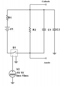
图 5 Gm-APD被动淬灭电路雪崩电压变化波形图
Figure 5. Gm-APD passive quenching circuit avalanche voltage change waveform

图 6 主动淬灭电路的原理图和仿真波形图
Figure 6. Schematic diagram and simulation waveform of active quenching circuit

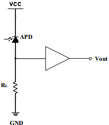
图 7 场效应管淬灭电路电路图以及等效模型
Figure 7. Circuit diagram and equivalent model of field effect transistor quenching circuit

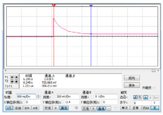
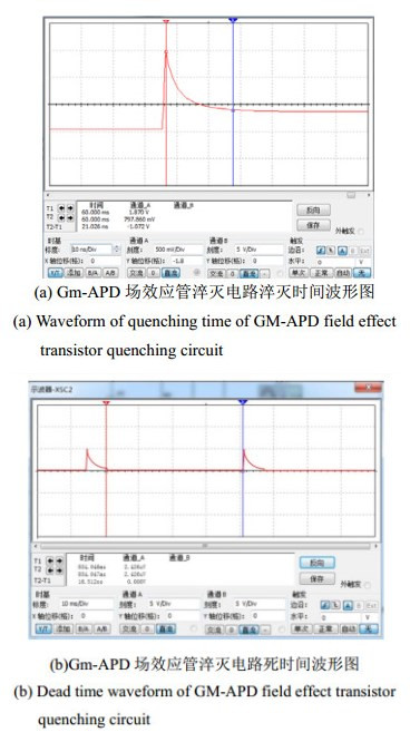
图 8 Gm-APD场效应管淬灭电路雪崩电压变化波形图
Figure 8. Gm-APD field effect transistor quenching circuit avalanche voltage change waveform
表 1 淬灭时间比较
Table 1. Quenching time comparison
Quenching mode Quenching time/ns Dead time/ns Passive quenching 1231 422.4 Active quenching 52.2 20 Field effect transistor quenching 21.026 16.5  下载: 导出CSV
-
[1] 王灿.面向雪崩光电二极管的光子计数读出电路设计[D].南京: 东南大学, 2017.WANG Can. Design of Photon Counting Readout Integrated Circuit for Avalanche Photondiode[D]. Nanjing: Southeast University, 2017. [2] 刘俊良, 李永富, 张春芳, 等.基于APD-PIN结电容平衡电路的门控单光子探测器[J].红外与激光工程, 2015, 44(11): 3181-3185. doi: 10.3969/j.issn.1007-2276.2015.11.003LIU Junliang, LI Yongfu, ZHANG Chunfang, et al. Single-photon detector based on GPQC with balanced APD-PIN junction capacitance[J]. Infrared and Laser Engineering, 2015, 44(11): 3181-3185. doi: 10.3969/j.issn.1007-2276.2015.11.003 [3] 郑丽霞.盖革模式雪崩光电二极管阵列读出电路的研究与实现[D].南京: 东南大学, 2017.ZHENG Lixia. Research and Implementation of GM-avalanche Photodiode Array Readout Dircuit[D]. Nanjing: Southeast University, 2017. [4] Haitz R H. Model for the electrical behavior of microplasma[J]. Journal of Applied Physics, 1964, 35(5): 1370-1376. doi: 10.1063/1.1713636 [5] Haitz R H. Mechanisms contributing to the noise pulse rate of avalanche diodes[J]. Journal of Applied Physics, 1965, 36(10): 3123-3131. doi: 10.1063/1.1702936 [6] Cova S, Longoni A, Andreoni A. Towards picoseconds resolution with single-photon avalanche diodes[J]. Review of Scientific Instruments, 1981, 52(3): 408-412. doi: 10.1063/1.1136594 [7] R H Haitz. Model for the electrical behavior of microplasma[J]. Journal of Applied Physics, 1964, 35(5): 1370-1376. doi: 10.1063/1.1713636 [8] Tisa S, Zappa F, Tosi A, et al. Electronics for single photon avalanche diode arrays[J]. Sensors and Actuators, 2007, 140(1): 113-122. doi: 10.1016/j.sna.2007.06.022 -


 点击查看大图

计量
- 文章访问数: 648
- HTML全文浏览量: 576
- PDF下载量: 120
- 被引次数: 0
